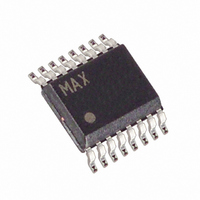
MAX6965AEE+ Maxim Integrated Products, MAX6965AEE+ Datasheet

MAX6965AEE+
Specifications of MAX6965AEE+
Related parts for MAX6965AEE+
MAX6965AEE+ Summary of contents
Page 1
... I Cs. ________________________________________________________________ Maxim Integrated Products For price, delivery, and to place orders, please contact Maxim Distribution at 1-888-629-4642, or visit Maxim’s website at www.maxim-ic.com. and Hot-Insertion Protection ♦ 400kbps, 2-Wire Serial Interface, 5.5V Tolerant ♦ 3.6V Operation ♦ Overall 8-Bit PWM LED Intensity Control ...
Page 2
LED Driver with Intensity Control and Hot-Insertion Protection ABSOLUTE MAXIMUM RATINGS Voltage (with respect to GND) V+ .............................................................................-0.3V to +4V SCL, SDA, AD0, BLINK, RST ...................................-0.3V to +6V O0–O8 ......................................................................-0.3V to +8V DC Current .....................................................55mA ...
Page 3
LED Driver with Intensity Control ELECTRICAL CHARACTERISTICS (continued) (Typical Operating Circuit 3.6V, T (Note 1) PARAMETER SYMBOL Output Low Voltage V O0–O8 Output Low-Voltage SDA V OLSDA PWM Clock Frequency f PWM TIMING CHARACTERISTICS (Typical ...
Page 4
LED Driver with Intensity Control and Hot-Insertion Protection TIMING CHARACTERISTICS (continued) (Typical Operating Circuit 3.6V, T (Note 1) PARAMETER RST Pulse Width Output Data Valid Note 1: All parameters tested +25°C. Specifications ...
Page 5
LED Driver with Intensity Control (T = +25°C, unless otherwise noted.) A SCOPE SHOT OF TWO OUTPUT PORTS MAX6965 toc07 MASTER INTENSITY SET TO 1/15 OUTPUT 1 2V/div OUTPUT 1 INDIVIDUAL INTENSITY SET TO 1/16 OUTPUT 2 2V/div OUTPUT ...
Page 6
LED Driver with Intensity Control and Hot-Insertion Protection Functional Overview The MAX6965 is a general-purpose output (GPO) peripheral that provides nine output ports, O0–O8, con- 2 trolled through an I C-compatible serial interface. All out- puts sink loads up ...
Page 7
LED Driver with Intensity Control The MAX6965 includes a register byte, which is avail- able as general-user RAM (Table 2). This byte is reset to the value 0xFF on power-up and when the RST input is taken low (Table ...
Page 8
LED Driver with Intensity Control and Hot-Insertion Protection 2 Table 1. MAX6965 I C Slave Address Map PIN AD0 A6 A5 SCL 1 SDA 1 GND Table 2. Register Address Map REGISTER Blink phase 0 outputs ...
Page 9
LED Driver with Intensity Control COMMAND BYTE IS STORED ON RECEIPT OF S SLAVE ADDRESS Figure 7. Command Byte Received HOW COMMAND BYTE AND DATA BYTE MAP INTO MAX6965's REGISTERS ACKNOWLEDGE FROM MAX6965 S SLAVE ADDRESS R/W Figure 8. ...
Page 10
LED Driver with Intensity Control and Hot-Insertion Protection Operation with Multiple Masters If the MAX6965 is operated on a 2-wire interface with multiple masters, a master reading the MAX6965 should use a repeated start between the write, which sets ...
Page 11
LED Driver with Intensity Control Table 3. Power-Up Configuration REGISTER FUNCTION POWER-UP CONDITION Blink phase 0 outputs User RAM Blink phase 1 outputs PWM oscillator is disabled; Master, O8 intensity O8 is high-impedance output; Configuration global intensity is enabled ...
Page 12
LED Driver with Intensity Control and Hot-Insertion Protection Table 4. Configuration Register (continued) REGISTER CONFIGURATION Write device configuration Read-back device configuration O8 output is low (blink is disabled) O8 output is high impedance (blink is disabled outp ...
Page 13
LED Driver with Intensity Control Table 6. Blink Phase 0 Register REGISTER Write outputs phase 0 Read-back outputs phase 0 Table 7. Blink Phase 1 Register REGISTER Write outputs phase 1 Read-back outputs phase 1 Table 8. PWM Application ...
Page 14
LED Driver with Intensity Control and Hot-Insertion Protection PWM Intensity Control The MAX6965 includes an internal oscillator, nominally 32kHz, to generate PWM timing for LED intensity control or other applications such as PWM trim DACs. PWM can be disabled ...
Page 15
LED Driver with Intensity Control Global/O8 Intensity Control The 4 bits used for output O8’s PWM individual intensity setting also double as the global intensity control (Table 11). Global intensity simplifies the PWM settings when the application requires them ...
Page 16
LED Driver with Intensity Control and Hot-Insertion Protection V is the supply voltage used to drive the LED (V). SUPPLY V is the forward voltage of the LED (V). LED V is the output low voltage of the MAX6964 ...
Page 17
LED Driver with Intensity Control Table 10. PWM Intensity Settings (Blink Enabled) PWM DUTY CYCLE OUTPUT CYCLE OUTPUT OUTPUT BLINK PHASE X BLINK PHASE X (OR REGISTER GLOBAL) BIT = 0 INTENSITY SETTING LOW HIGH LOW TIME TIME TIME ...
Page 18
LED Driver with Intensity Control and Hot-Insertion Protection Table 11. Master, O8 Intensity Register REGISTER MASTER AND GLOBAL INTENSITY Write master and global intensity Read-back master and global intensity Master intensity duty cycle is 0/15 (off); internal oscillator is ...
Page 19
LED Driver with Intensity Control Table 12. Output Intensity Registers REGISTER OUTPUTS O1, O0 INTENSITY Write output O1, O0 intensity Read-back output O1, O0 intensity Output O1 intensity duty cycle is 1/16 Output O1 intensity duty cycle is 2/16 ...
Page 20
LED Driver with Intensity Control and Hot-Insertion Protection TOP VIEW BLINK 1 RST 2 ADO MAX6965AEE GND 8 QSOP 20 ______________________________________________________________________________________ TOP VIEW SDA 14 SCL 13 ...
Page 21
LED Driver with Intensity Control (The package drawing(s) in this data sheet may not reflect the most current specifications. For the latest package outline information www.maxim-ic.com/packages.) ______________________________________________________________________________________ and Hot-Insertion Protection PACKAGE OUTLINE, QSOP .150", .025" LEAD PITCH ...
Page 22
... Maxim cannot assume responsibility for use of any circuitry other than circuitry entirely embodied in a Maxim product. No circuit patent licenses are implied. Maxim reserves the right to change the circuitry and specifications without notice at any time. 22 ____________________Maxim Integrated Products, 120 San Gabriel Drive, Sunnyvale, CA 94086 408-737-7600 © 2005 Maxim Integrated Products Package Information (continued) ...


