LM2751SD-B/NOPB National Semiconductor, LM2751SD-B/NOPB Datasheet - Page 4
LM2751SD-B/NOPB
Manufacturer Part Number
LM2751SD-B/NOPB
Description
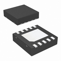
IC LED DRIVR WHITE BCKLGT 10-LLP
Manufacturer
National Semiconductor
Type
Backlight, White LEDr
Datasheet
1.LM2751SD-ANOPB.pdf
(11 pages)
Specifications of LM2751SD-B/NOPB
Topology
PWM, Switched Capacitor (Charge Pump)
Number Of Outputs
1
Internal Driver
Yes
Type - Primary
Backlight
Type - Secondary
White LED
Frequency
725kHz
Voltage - Supply
2.8 V ~ 5.5 V
Voltage - Output
4.5V
Mounting Type
Surface Mount
Package / Case
10-LLP
Operating Temperature
-40°C ~ 85°C
Current - Output / Channel
150mA
Internal Switch(s)
Yes
Efficiency
90%
Lead Free Status / RoHS Status
Lead free / RoHS Compliant
Other names
LM2751SD-B
LM2751SD-BTR
LM2751SD-BTR
Available stocks
Company
Part Number
Manufacturer
Quantity
Price
Company:

Part Number:
LM2751SD-B/NOPB
Manufacturer:
NS
Quantity:
7 708


www.national.com
fsw
V
V
I
I
V
I
t
IH
IL
SC
ON
Symbol
IH
IL
G
Electrical Characteristics
Limits in standard typeface are for T
(-40˚C ≤ T
= 3.6V, V(EN) = V
Note 1: Absolute Maximum Ratings indicate limits beyond which damage to the component may occur. Operating Ratings are conditions under which operation of
the device is guaranteed. Operating Ratings do not imply guaranteed performance limits. For guaranteed performance limits and associated test conditions, see the
Electrical Characteristics tables.
Note 2: All voltages are with respect to the potential at the GND pin.
Note 3: Internal thermal shutdown circuitry protects the device from permanent damage. Thermal shutdown engages at T
T
Note 4: The Human body model is a 100 pF capacitor discharged through a 1.5kΩ resistor into each pin. The machine model is a 200pF capacitor discharged
directly into each pin. MIL-STD-883 3015.7
Note 5: In applications where high power dissipation and/or poor package thermal resistance is present, the maximum ambient temperature may have to be
derated. Maximum ambient temperature (T
dissipation of the device in the application (P
following equation: T
Note 6: Junction-to-ambient thermal resistance (θ
standard JESD51-7. The test board is a 4 layer FR-4 board measuring 102mm x 76mm x 1.6mm with a 2 x 1 array of thermal vias. The ground plane on the board
is 50mm x 50mm. Thickness of copper layers are 36µm/18µm /18µm/36µm (1.5oz/1oz/1oz/1.5oz). Ambient temperature in simulation is 22
dissipation is 1W.
The value of θ
conditions. In applications where high maximum power dissipation exists (high V
information on these topics, please refer to Application Note 1187: Leadless Leadframe Package (LLP) and the Power Efficiency and Power Dissipation
section of this datasheet.
Note 7: Min and Max limits are guaranteed by design, test, or statistical analysis. Typical numbers are not guaranteed, but represent the most likely norm.
Note 8: C
Note 9: EN Logic Input High Current (I
Note 10: Turn-on time is measured from when the EN signal is pulled high until the output voltage on V
J
=140˚C (typ.).
IN
Switching Frequency
Logic Input High
Logic Input Low
Logic Input High Current
Logic Input Low Current
Gain Transition Voltage
(Version A, B)
Short Circuit Output
Current
V
(Note 10)
, C
A
OUT
JA
OUT
≤ +85˚C) . Unless otherwise noted, specifications apply to the LM2751 Typical Application Circuit (pg. 1) with: V
of the LM2751 in LLP-10 could fall in a range as wide as 50
, C
Turn-On Time
A-MAX
Parameter
1
, and C
IN,
CS0 = CS1 = V
= T
J-MAX-OP
2
: Low-ESR Surface-Mount Ceramic Capacitors (MLCCs) used in setting electrical characteristics.
IH
- (θ
) is due to a 1MΩ(typ.) pull-down resistor connected internally between the EN pin and GND.
JA
A-MAX
D-MAX
x P
A
IN
CS0 = High, CS1 = Low
2.8V ≤ V
CS0 = Low, CS1 = Low
2.8V ≤ V
CS0 = Low, CS1 = High
2.8V ≤ V
CS0 = High, CS1 = High
2.8V ≤ V
Input Pins: EN, CS0, CS1
2.8V ≤ V
Input Pins: EN, CS0, CS1
2.8V ≤ V
Input Pins: CS0, CS1
V(CSx) = 1.8V
Input Pin: EN
V(EN) = 1.8V(Note 9)
Input Pins: EN, CS0, CS1
V(EN, CSx) = 0V
1.5X to 2X
2X to 1.5X
Hysteresis
V
= 25
OUT
, C
D-MAX
JA
) is dependent on the maximum operation junction temperature (T
), and the junction-to ambient thermal resistance of the part/package in the application (θ
) is taken from a thermal modeling result, performed under the conditions and guidelines set forth in the JEDEC
1
o
= 0V
= C
).
C. Limits in boldface type apply over the full operating ambient temperature range
(Notes 2, 7) (Continued)
IN
IN
IN
IN
IN
IN
2
≤ 5.5V
≤ 5.5V
≤ 5.5V
≤ 5.5V
≤ 5.5V
≤ 5.5V
= 1.0µF, C
Conditions
o
IN
C/W to 150
= C
4
IN
, high I
OUT
o
C/W (if not wider), depending on PWB material, layout, and environmental
= 2.2µF (Note 8).
OUT
), special care must be paid to thermal dissipation issues. For more
OUT
crosses 90% of its final value.
(−30%)
(−30%)
(−30%)
(−30%)
1.00
Min
210
508
6.7
26
40
0
J-MAX-OP
J
3.50
3.58
Typ
300
725
250
300
=150˚C (typ.) and disengages at
9.5
37
10
10
80
2
= 115
o
C), the maximum power
(+30%)
(+30%)
(+30%)
(+30%)
Max
12.3
390
942
150
JA
V
.30
48
o
), as given by the
IN
C, still air. Power
Units
kHz
mV
mA
nA
µA
nA
µs
V
V
V
IN
Related parts for LM2751SD-B/NOPB
Image
Part Number
Description
Manufacturer
Datasheet
Request
R

Part Number:
Description:
IC LED DRIVR WHITE BCKLGT 10-LLP
Manufacturer:
National Semiconductor
Datasheet:

Part Number:
Description:
IC,Laser Diode/LED Driver,LLCC,10PIN,PLASTIC
Manufacturer:
National Semiconductor
Part Number:
Description:
IC,Laser Diode/LED Driver,LLCC,10PIN,PLASTIC
Manufacturer:
National Semiconductor
Part Number:
Description:
National Semiconductor [8-Bit D/A Converter]
Manufacturer:
National Semiconductor
Datasheet:
Part Number:
Description:
National Semiconductor [Media Coprocessor]
Manufacturer:
National Semiconductor
Datasheet:
Part Number:
Description:
Digitally Controlled Tone and Volume Circuit with Stereo Audio Power Amplifier, Microphone Preamp Stage and National 3D Sound
Manufacturer:
National Semiconductor
Datasheet:
Part Number:
Description:
Digitally Controlled Tone and Volume Circuit with Stereo Audio Power Amplifier, Microphone Preamp Stage and National 3D Sound
Manufacturer:
National Semiconductor
Datasheet:
Part Number:
Description:
AC97 Rev 2 Codec with Sample Rate Conversion and National 3D Sound
Manufacturer:
National Semiconductor
Part Number:
Description:
Manufacturer:
National Semiconductor
Datasheet:
Part Number:
Description:
Manufacturer:
National Semiconductor
Datasheet:
Part Number:
Description:
General Purpose, Low Voltage, Low Power, Rail-to-Rail Output Operational Amplifiers
Manufacturer:
National Semiconductor
Datasheet:
Part Number:
Description:
8-bit 20 MSPS flash A/D converter.
Manufacturer:
National Semiconductor
Datasheet:
Part Number:
Description:
Low Noise Quad Operational Amplifier
Manufacturer:
National Semiconductor
Datasheet:
Part Number:
Description:
Quad Differential Line Receivers
Manufacturer:
National Semiconductor
Datasheet: