CAT3612HV2-T2 ON Semiconductor, CAT3612HV2-T2 Datasheet - Page 8
CAT3612HV2-T2
Manufacturer Part Number
CAT3612HV2-T2
Description
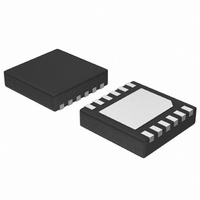
IC LED DRVR PHOTO FLASH 12-TDFN
Manufacturer
ON Semiconductor
Type
Photo Flash LEDr
Datasheet
1.CAT3612HV2-T2.pdf
(13 pages)
Specifications of CAT3612HV2-T2
Topology
Switched Capacitor (Charge Pump)
Number Of Outputs
2
Internal Driver
Yes
Type - Primary
Flash/Torch
Frequency
800kHz ~ 1.3MHz
Voltage - Supply
3 V ~ 5.5 V
Mounting Type
Surface Mount
Package / Case
12-VFDFN Exposed Pad
Operating Temperature
-40°C ~ 85°C
Current - Output / Channel
150mA
Internal Switch(s)
Yes
Efficiency
90%
Number Of Segments
2
Operating Supply Voltage
3 V to 5.5 V
Maximum Operating Temperature
+ 85 C
Mounting Style
SMD/SMT
Minimum Operating Temperature
- 40 C
Lead Free Status / RoHS Status
Lead free / RoHS Compliant
Voltage - Output
-
Lead Free Status / Rohs Status
Details
Other names
3612HV2-T2
CAT3612HV2-T2TR
CAT3612HV2-T2TR


3. LED1, LED2 pins should not be left floating. They should be connected to the LED cathode, or tied to the VOUT pin if not used.
Pin Function
VIN is the supply pin for the device. A small 1 mF ceramic
bypass capacitor is required between the VIN pin and
ground near the device. The operating input voltage range is
up to 5.5 V. When the input supply falls below the
undervoltage threshold (2 V), all LEDs channels are
disabled.
EN/DIM is the enable and dimming control logic input for
all LED channels. Guaranteed levels of logic high and logic
low are set at 1.3 V and 0.4 V respectively. When EN/DIM
is initially taken high, the device becomes enabled and the
LED currents remain at 0 mA. The falling edge of the first
pulse on EN/DIM sets the LED currents to the full scale
150 mA.
the LED current decreases by 150/31 mA. On the 32
the LED current is set to zero. The next pulse on EN/DIM
resets the current back to full scale 150 mA.
EN/DIM pin must be held low for 1.5 ms or more.
Table 5. PIN DESCRIPTIONS
On each consecutive falling edge of the pulse on EN/DIM,
To place the device into zero current shutdown mode, the
Pin #
TAB
10
11
12
1
2
3
4
5
6
7
8
9
EN/DIM
Name
VOUT
LED1
LED2
GND
C1+
C2+
TAB
C1−
C2−
VIN
−
−
Supply voltage.
Bucket capacitor 1 terminal
Bucket capacitor 1 terminal
Bucket capacitor 2 terminal
Ground reference
LED1 cathode terminal (if not used, connect to VOUT) (Note 3)
LED2 cathode terminal (if not used, connect to VOUT) (Note 3)
Bucket capacitor 2 terminal
Not connected
Device enable (active high) and dimming control input.
Not connected
Charge pump output connected to the LED anodes.
Connect to GND on the PCB.
nd
http://onsemi.com
pulse,
8
VOUT is the charge pump output that is connected to the
LED anodes. A small 1 mF ceramic bypass capacitor is
required between the VOUT pin and ground near the device.
GND is the ground reference for the charge pump. The pin
must be connected to the ground plane on the PCB.
C1+, C1− are connected to each side of the 1 mF ceramic
bucket capacitor C1.
C2+, C2− are connected to each side of the 1 mF ceramic
bucket capacitor C2.
LED1, LED2 provide the internal regulated current for each
of the LED cathodes. These pins enter a high impedance
zero current state whenever the device is in shutdown mode.
In applications using only one LED channel, the unused
channel should be tied directly to VOUT. The disabled
channel only draws about 0.5 mA.
TAB is the exposed pad underneath the package. For best
thermal performance, the tab should be soldered to the PCB
and connected to the ground plane.
Function
Related parts for CAT3612HV2-T2
Image
Part Number
Description
Manufacturer
Datasheet
Request
R

Part Number:
Description:
ON Semiconductor [VOLTAGE REGULATOR]
Manufacturer:
ON Semiconductor
Datasheet:
Part Number:
Description:
357-036-542-201 CARDEDGE 36POS DL .156 BLK LOPRO
Manufacturer:
ON Semiconductor
Datasheet:
Part Number:
Description:
357-036-542-201 CARDEDGE 36POS DL .156 BLK LOPRO
Manufacturer:
ON Semiconductor
Datasheet:
Part Number:
Description:
357-036-542-201 CARDEDGE 36POS DL .156 BLK LOPRO
Manufacturer:
ON Semiconductor
Datasheet:
Part Number:
Description:
357-036-542-201 CARDEDGE 36POS DL .156 BLK LOPRO
Manufacturer:
ON Semiconductor
Datasheet:
Part Number:
Description:
357-036-542-201 CARDEDGE 36POS DL .156 BLK LOPRO
Manufacturer:
ON Semiconductor
Datasheet:
Part Number:
Description:
357-036-542-201 CARDEDGE 36POS DL .156 BLK LOPRO
Manufacturer:
ON Semiconductor
Datasheet:
Part Number:
Description:
357-036-542-201 CARDEDGE 36POS DL .156 BLK LOPRO
Manufacturer:
ON Semiconductor
Datasheet:
Part Number:
Description:
357-036-542-201 CARDEDGE 36POS DL .156 BLK LOPRO
Manufacturer:
ON Semiconductor
Datasheet:
Part Number:
Description:
357-036-542-201 CARDEDGE 36POS DL .156 BLK LOPRO
Manufacturer:
ON Semiconductor
Datasheet:
Part Number:
Description:
357-036-542-201 CARDEDGE 36POS DL .156 BLK LOPRO
Manufacturer:
ON Semiconductor
Datasheet:
Part Number:
Description:
Manufacturer:
ON Semiconductor
Datasheet:
Part Number:
Description:
Manufacturer:
ON Semiconductor
Datasheet:
Part Number:
Description:
Manufacturer:
ON Semiconductor
Datasheet: