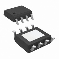
LM3404HVMR/NOPB National Semiconductor, LM3404HVMR/NOPB Datasheet - Page 18

LM3404HVMR/NOPB
Manufacturer Part Number
LM3404HVMR/NOPB
Description
IC LED DRVR HP CONST CURR 8-PSOP
Manufacturer
National Semiconductor
Series
PowerWise®r
Type
High Power, Constant Currentr
Specifications of LM3404HVMR/NOPB
Constant Current
Yes
Topology
PWM, Step-Down (Buck)
Number Of Outputs
1
Internal Driver
Yes
Type - Primary
Automotive
Type - Secondary
High Brightness LED (HBLED), White LED
Frequency
1MHz
Voltage - Supply
6 V ~ 75 V
Mounting Type
Surface Mount
Package / Case
8-PSOP
Operating Temperature
-40°C ~ 125°C
Current - Output / Channel
1A
Internal Switch(s)
Yes
Efficiency
96%
Current, Input Bias
0.1 μA
Current, Output
1.2 A
Current, Supply
625 μA
Package Type
PSOP
Regulator Type
Buck (Step-Down), Switching
Temperature, Operating, Range
-40 to +125 °C
Time, Fall
20 ns
Time, Rise
20 ns
Voltage, Input
6 to 75 V
Voltage, Output
7 V
For Use With
551600000-001A/NOPB - BOARD WEBENCH SO8/SOP LM3404/2LM3404HVEVAL - BOARD EVALUATION LM3404HV
Lead Free Status / RoHS Status
Lead free / RoHS Compliant
Voltage - Output
-
Lead Free Status / Rohs Status
RoHS Compliant part
Electrostatic Device
Other names
LM3404HVMR
Available stocks
Company
Part Number
Manufacturer
Quantity
Price
Company:
Part Number:
LM3404HVMR/NOPB
Manufacturer:
TI
Quantity:
4 450
Part Number:
LM3404HVMR/NOPB
Manufacturer:
TI/德州仪器
Quantity:
20 000
www.national.com
VIN PIN PROTECTION
The VIN pin also has an ESD structure from the pin to GND
with a breakdown voltage of approximately 80V. Any transient
that exceeds this voltage may damage the device. Although
transient absorption is usually present at the front end of a
switching converter circuit, damage to the VIN pin can still
occur.
When V
charge C
circuit board trace inductance as shown in
cited trace inductance then resonates with the input capaci-
tance (similar to an under-damped LC tank circuit) and
causes voltages at the VIN pin to rise well in excess of both
V
IN
and the voltage at the module input connector as clamped
IN
IN
is hot swapped in, the current that rushes in to
up to the V
IN
value also charges (energizes) the
FIGURE 10. VIN Pin with Typical Input Protection
Figure
10. The ex-
18
by the input TVS. If the resonating voltage at the VIN pin ex-
ceeds the 80V breakdown voltage of the ESD structure, the
ESD structure will activate and then “snap-back” to a lower
voltage due to its inherent design. If this lower snap-back
voltage is less than the applied nominal V
nificant current will flow through the ESD structure resulting
in the IC being damaged.
An additional TVS or small zener diode should be placed as
close as possible to the VIN pins of each IC on the board, in
parallel with the input capacitor as shown in
nor amount of series resistance in the input line would also
help, but would lower overall conversion efficiency. For this
reason, NTC resistors are often used as inrush limiters in-
stead.
20205461
IN
voltage, then sig-
Figure
11. A mi-


