LM2753SD/NOPB National Semiconductor, LM2753SD/NOPB Datasheet - Page 8
LM2753SD/NOPB
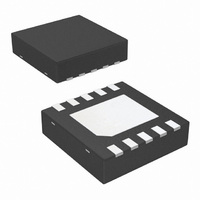
Manufacturer Part Number
LM2753SD/NOPB
Description
IC LED DRIVER PHOTO FLASH 10-LLP
Manufacturer
National Semiconductor
Type
Photo Flash LEDr
Datasheet
1.LM2753SDNOPB.pdf
(12 pages)
Specifications of LM2753SD/NOPB
Topology
PWM, Switched Capacitor (Charge Pump)
Number Of Outputs
1
Internal Driver
Yes
Type - Primary
Flash/Torch
Type - Secondary
White LED
Frequency
725kHz
Voltage - Supply
3 V ~ 5.5 V
Voltage - Output
5V
Mounting Type
Surface Mount
Package / Case
10-LLP
Operating Temperature
-40°C ~ 85°C
Current - Output / Channel
250mA
Internal Switch(s)
Yes
Lead Free Status / RoHS Status
Lead free / RoHS Compliant
Efficiency
-
Other names
LM2753SD
LM2753SDTR
LM2753SDTR


www.national.com
ered to the output in order to keep the output voltage in
regulation. When the output voltage is above the target reg-
ulation voltage the part idles, consuming minimal supply cur-
rent with C
disconnected from V
plied solely by the charge stored on the output capacitor. As
this capacitor discharges and the output voltage falls below
the target regulation voltage, the charge pump activates, and
charge is delivered to the output. This charge supplies the
load current and boosts the voltage on the output capacitor.
The primary benefit of PFM regulation is when output currents
are light and the part is predominantly in the low-supply-cur-
rent idle state. Net supply current is minimal because the part
only occasionally needs to recharge the output capacitor by
activating the charge pump. With PFM regulation, input and
output ripple frequencies vary significantly, and are depen-
dent on output current, input voltage, and to a lesser degree,
other factors such as temperature, internal switch character-
istics, and capacitor characteristics (voltage tolerance, tem-
perature variation).
OUTPUT VOLTAGE RIPPLE
The voltage ripple on the output of the LM2753 is highly de-
pendent on the application conditions. The output capaci-
tance, input voltage, and output current each play a significant
part in determining the output voltage ripple. Due to the com-
plexity of the LM2753 operation, providing equations or mod-
els to approximate the magnitude of the ripple cannot be
easily accomplished. However, the following general state-
ments can be made.
The output capacitor will have a significant effect on output
voltage ripple magnitude. Ripple magnitude will typically be
linearly proportional to the output capacitance present. The
ESR of the output capacitor also contributes to the output
voltage ripple, as there is effectively an AC voltage drop
across the ESR due to current switching in and out of the ca-
pacitor. To keep the voltage ripple small, a low-ESR ceramic
capacitor is recommended on the output. Placing multiple ca-
pacitors in parallel can reduce ripple significantly, by both
increasing capacitance and reducing ESR. When capacitors
are in parallel the ESR of the capacitors are in parallel as well,
resulting in a net ESR according to the properties of parallel
resistance. Two identical capacitors in parallel have twice the
capacitance and half the ESR as compared to a single ca-
pacitor if the same type. On a similar note, if a large-value,
high-ESR capacitor (tantalum, for example) is to be used as
the primary output capacitor, the net ESR can be significantly
reduced by placing a low-ESR ceramic capacitor in parallel
with this primary output capacitor.
I
An internal FET is connected between the V
I
the Flash input pin, the internal FET turns on and connects
I
to be used, the Flash input pin can be tied to GND and the
I
In the typical application circuit there is one resistor between
V
Flash LED. When a LOW logic signal is placed on the Flash
input pin, the internal FET opens and current flows from
V
a logic HIGH signal is applied to the Flash input pin the inter-
nal FET closes, shorting out the resistor between V
I
Flash LED.
OUT
OUT
OUT
OUT
OUT
OUT
OUT
, and current flows through the second resistor and the
pin of the LM2753. When a logic high signal is placed on
to V
PIN
pin can be left unconnected.
through both resistors and through the Flash LED. When
and I
OUT
1
OUT
in less than 10ns (typ). If the I
is connected between V
and another resistor between I
OUT
. In this state, the load current is sup-
IN
and GND and V
OUT
OUT
pin is not going
OUT
pin and the
and the
OUT
IN
and
is
8
Follow the steps below to set the desired current levels for the
Flash LED:
Setting Flash Current
1.
2.
3.
Setting Torch Current
1.
2.
3.
4.
5.
PWM BRIGHTNESS CONTROL PROCEDURES
The brightness of a Flash LED connected to V
early varied from zero up to the maximum programmed cur-
rent level by applying a Pulse-Width-Modulated signal to the
EN pin of the LM2753. The following procedures illustrate how
to program the LED drive current and adjust the output current
level using a PWM signal.
1.
2.
MULTI-LEVEL SWITCH ARRAY.
In order to supply high load currents across the entire V
erating range, especially at lower V
pump are normally designed to have low on-resistance. How-
ever at high input voltages and low load currents, this low
resistance results in high output voltage ripple due to the out-
put capacitor being charged too quickly. To solve this prob-
lem, while still being able to deliver the needed output current,
Determine the LED's forward voltage at the desired Flash
current.
Find the voltage difference between I
forward voltage.
Divide the voltage difference by the desired Flash current
to obtain the needed Flash LED ballast resistance
First determine required Flash Ballast
Determine the LED's forward voltage at the desired
continuous Torch current
Find the voltage difference between V
forward voltage.
Divide the voltage difference by the desired Torch current
to obtain the total resistance needed.
Subtract the Flash Ballast resistance from this total
resistance to find the required Torch resistance between
V
To select the maximum desired current level, refer to the
"I
"Setting Flash Current" and "Setting Torch Current"
subheadings.
Brightness control for "Torch" mode can be implemented
by pulsing a signal at the EN pin, while Flash is connected
to a logic LOW signal. Also, brightness control can also
be implemented for Flash mode by pulsing a signal on
the Flash pin while the part is already enabled (EN = logic
HIGH). LED brightness is proportional to the duty cycle
(D) of the PWM signal. For linear brightness control over
the full duty cycle adjustment range, the PWM frequency
(f) should be limited during Torch mode to accommodate
the turn-on time (T
PWM frequency should be limited during "Flash" mode
to accommodate the turn-on time (T
I
If the PWM frequency is much less than 100Hz, flicker
may be seen in the LEDs. For the LM2753, zero duty
cycle will turn off the LED and a 50% duty cycle will result
in an average I
current. For example, if the output is programmed for a
maximum of 100mA through the Flash LED, a 50% duty
cycle will result in an average I
OUT
OUT
OUT
output FET.
Pin" section and follow the steps detailed in the
and I
OUT
OUT
f
MAX
D × (1/f) > T
ON
being half of the programmed LED
= D
= 640µs) of the device. Also, the
MIN
÷ T
ON,FLASH
LED
IN
ON,FLASH
, switches in the charge
of 50mA.
FLASH
OUT
OUT
and the LED
OUT
= 10ns) of the
and the LED
can be lin-
IN
op-
Related parts for LM2753SD/NOPB
Image
Part Number
Description
Manufacturer
Datasheet
Request
R

Part Number:
Description:
IC,Laser Diode/LED Driver,LLCC,10PIN,PLASTIC
Manufacturer:
National Semiconductor
Part Number:
Description:
National Semiconductor [8-Bit D/A Converter]
Manufacturer:
National Semiconductor
Datasheet:
Part Number:
Description:
National Semiconductor [Media Coprocessor]
Manufacturer:
National Semiconductor
Datasheet:
Part Number:
Description:
Digitally Controlled Tone and Volume Circuit with Stereo Audio Power Amplifier, Microphone Preamp Stage and National 3D Sound
Manufacturer:
National Semiconductor
Datasheet:
Part Number:
Description:
Digitally Controlled Tone and Volume Circuit with Stereo Audio Power Amplifier, Microphone Preamp Stage and National 3D Sound
Manufacturer:
National Semiconductor
Datasheet:
Part Number:
Description:
AC97 Rev 2 Codec with Sample Rate Conversion and National 3D Sound
Manufacturer:
National Semiconductor
Part Number:
Description:
Manufacturer:
National Semiconductor
Datasheet:
Part Number:
Description:
Manufacturer:
National Semiconductor
Datasheet:
Part Number:
Description:
General Purpose, Low Voltage, Low Power, Rail-to-Rail Output Operational Amplifiers
Manufacturer:
National Semiconductor
Datasheet:
Part Number:
Description:
8-bit 20 MSPS flash A/D converter.
Manufacturer:
National Semiconductor
Datasheet:
Part Number:
Description:
Low Noise Quad Operational Amplifier
Manufacturer:
National Semiconductor
Datasheet:
Part Number:
Description:
Quad Differential Line Receivers
Manufacturer:
National Semiconductor
Datasheet:
Part Number:
Description:
Quad High Speed Trapezoidal? Bus Transceiver
Manufacturer:
National Semiconductor
Datasheet:
Part Number:
Description:
Dual Line Receiver
Manufacturer:
National Semiconductor
Datasheet: