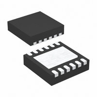
LT3498EDDB#TRMPBF Linear Technology, LT3498EDDB#TRMPBF Datasheet - Page 15

LT3498EDDB#TRMPBF
Manufacturer Part Number
LT3498EDDB#TRMPBF
Description
IC LED DRVR WT/OLED BCKLGT 12DFN
Manufacturer
Linear Technology
Type
Backlight, OLED, White LEDr
Datasheet
1.LT3498EDDBTRMPBF.pdf
(24 pages)
Specifications of LT3498EDDB#TRMPBF
Topology
PWM, Step-Up (Boost)
Number Of Outputs
1
Internal Driver
Yes
Type - Primary
Backlight
Type - Secondary
OLED, White LED
Frequency
1.8MHz ~ 2.8MHz
Voltage - Supply
2.5 V ~ 12 V
Voltage - Output
32V
Mounting Type
Surface Mount
Package / Case
12-DFN
Operating Temperature
-40°C ~ 85°C
Current - Output / Channel
20mA
Internal Switch(s)
Yes
No. Of Outputs
2
Output Current
200mA
Output Voltage
32V
Input Voltage
2.5V To 12V
Dimming Control Type
PWM / DC
Operating Temperature Range
-40°C To +85°C
Driver Case Style
DFN
Rohs Compliant
Yes
Lead Free Status / RoHS Status
Lead free / RoHS Compliant
Efficiency
-
Other names
LT3498EDDB#TRMPBFTR
Available stocks
Company
Part Number
Manufacturer
Quantity
Price
APPLICATIONS INFORMATION— OLED DRIVER
a soft transition occurs between the CTRL2 pin and the
internal reference. Figure 10 shows this behavior.
To set the maximum output voltage, select the values of
R
When CTRL2 is used to override the internal reference,
the output voltage can be lowered from the maximum
value down to nearly the input voltage level. If the volt-
age source driving the CTRL2 pin is located at a distance
to the LT3498, a small 0.1μF capacitor may be needed to
bypass the pin locally.
FB2
R
FB2
according to the following equation:
=182 •
CAP1
CAP1
LED1
LED1
1.500
1.250
0.250
1.000
0.750
0.500
Figure 10. CTRL2 to FB2 Transfer Curve
Figure 11. Feedback Connection Using
the CAP2 Pin or the V
0
0
CTRL1
CTRL1
SW1
SW1
V
1.215
0.3
OUT2
GND1
GND1
V
V
IN
IN
LT3498
LT3498
CTRL2 VOLTAGE (V)
0.5
– 1 , k
SW2
GND2
SW2
GND2
0.8
OUT2
CAP2
CTRL2
CAP2
CTRL2
1.0
Pin
V
V
OUT2
OUT2
FB2
FB2
C2
1.3
3498 F10
R
R
1.5
FB2
FB2
3498 F11
C2
C3
Choosing a Feedback Node
The single feedback resistor may be connected to the V
pin or to the CAP2 pin (see Figure 11). Regulating the
V
voltage drop across the output disconnect PMOS. Regu-
lating the CAP2 pin does not compensate for the voltage
drop across the output disconnect, resulting in an output
voltage V
the resistor divider. Under most conditions, it is advised
that the feedback resistor be tied to the V
Connecting the Load to the CAP2 Node
The effi ciency of the converter can be improved by con-
necting the load to the CAP2 pin instead of the V
The power loss in the PMOS disconnect circuit is then
made negligible. By connecting the feedback resistor to
the V
in the feedback resistor string during shutdown since
the PMOS transistor will be open (see Figure 12). The
disadvantage of this method is that the CAP2 node can-
not go to ground during shutdown, but will be limited to
around a diode drop below V
part should only sink current. Never force external power
supplies onto the CAP2 or V
output capacitor should be placed on the node to which
the load is connected.
OUT2
CAP1
LED1
OUT2
pin eliminates the output offset resulting from the
CTRL1
SW1
OUT2
pin, no quiescent current will be consumed
GND1
that is slightly lower than the voltage set by
V
Figure 12. Improved Effi ciency
IN
LT3498
GND2
SW2
CAP2
CTRL2
OUT2
IN
V
. Loads connected to the
OUT2
FB2
3498 F12
pins. The larger value
R
FB2
OUT2
LT3498
C3
pin.
OUT2
15
OUT2
I
3498fa
pin.
LOAD


