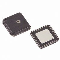
ADN2848ACP-32-RL Analog Devices Inc, ADN2848ACP-32-RL Datasheet - Page 8

ADN2848ACP-32-RL
Manufacturer Part Number
ADN2848ACP-32-RL
Description
IC DVR LASER DIODE 3V 32-LFCSP
Manufacturer
Analog Devices Inc
Type
Laser Diode Driver (Fiber Optic)r
Datasheet
1.ADN2848ACPZ-32-RL.pdf
(12 pages)
Specifications of ADN2848ACP-32-RL
Number Of Channels
1
Rohs Status
RoHS non-compliant
Data Rate
1.25Gbps
Voltage - Supply
3 V ~ 3.6 V
Current - Supply
50mA
Current - Modulation
80mA
Current - Bias
100mA
Operating Temperature
-40°C ~ 85°C
Package / Case
32-VFQFN, CSP Exposed Pad
Mounting Type
Surface Mount
Operating Supply Voltage (min)
3V
Mounting
Surface Mount
Lead Free Status / RoHS Status
Not Compliant
ADN2848
Example:
*The smallest valid value for R
The laser degrade alarm, DEGRADE, is provided to give a
warning of imminent laser failure if the laser diode degrades
further or if environmental conditions such as increasing
temperature continue to stress the LD.
The laser fail alarm, FAIL, is activated when the transmitter can
no longer be guaranteed to be SONET/SDH compliant. This
occurs when one of the following conditions arise:
DEGRADE is raised only when the bias current exceeds 90% of
ASET current.
MONITOR CURRENTS
IBMON, IMMON, and IMPDMON are current controlled
current sources from V
and MPD current for increased monitoring functionality. An
external resistor to GND gives a voltage proportional to the
current monitored.
If the monitoring function IMPDMON is not required, the
IMPD pin must be grounded and the monitor photodiode
output must be connected directly to the PSET pin.
DATA AND CLOCK INPUTS
Data and clock inputs are ac-coupled (10 nF capacitors
recommended) and terminated via a 100 Ω internal resistor
between DATAP and DATAN and also between the CLKP and
CLKN pins. There is a high impedance circuit to set the
common-mode voltage, which is designed to allow for
maximum input voltage headroom over temperature. It is
necessary that ac coupling be used to eliminate the need for
matching between common-mode voltages.
I
BIAS
maximum of 100 μA.
•
•
I
I
R
FAIL
ASET
ASET
The ASET threshold is reached.
The ALS pin is set high. This shuts off the modulation
and bias currents to the LD, resulting in the MPD
current dropping to zero. This gives closed-loop
feedback to the system that ALS has been enabled.
=
=
*
50
=
I
100
FAIL
1
mA
I
2 .
ASET
=
V
so
50
=
100
I
CC
DEGRADE
500
mA
ASET
. They mirror the bias, modulation,
1
2 .
is 1.2 kΩ, because this corresponds to the
μA
=
500
=
=
45
2
μA
4 .
mA
kΩ
Rev. A | Page 8 of 12
For input signals that exceed 500 mV p-p single-ended, it is
necessary to insert an attenuation circuit as shown in Figure 6.
CCBIAS
When the laser is used in ac-coupled mode, the CCBIAS pin
and the I
mode, CCBIAS is tied to V
I
To achieve optimum optical eye quality, a pull-up resistor R
shown in Figure 8 and Figure 9, is required. The recommended
R
AUTOMATIC LASER SHUTDOWN
The ADN2848 ALS allows compliance to ITU-T-G958 (11/94),
section 9.7. When ALS is logic high, both the bias and the
modulation currents are turned off. Correct operation of ALS is
confirmed by the FAIL alarm being raised when ALS is
asserted. Note that this is the only time that DEGRADE is low
while FAIL is high.
ALARM INTERFACES
The FAIL and DEGRADE outputs have an internal 30 kΩ pull-
up resistor that is used to pull the digital high value to V
However, the alarm output can be overdriven with an external
resistor, allowing alarm interfacing to non-V
alarm output levels must be below the V
ADN2848.
BIAS
Z
value is approximately 200 Ω ~ 500 Ω.
BIAS
DATAN
DATAP
pin are tied together (see Figure 9). In dc-coupled
NOTE THAT R
INPUT IMPEDANCE OF THE ADN2848.
R1
R2
Figure 5. AC Coupling of Data Inputs
R3
Figure 6. Attenuation Circuit
IN
DATAN/CLKN
DATAP/CLKP
= 100Ω = THE DIFFERENTIAL
50Ω
CC
.
50Ω
ADN2848
V
REG
R
R = 2.5kΩ, DATA
R = 3kΩ, CLK
TO FLIP-FLOPS
400µA TYP
ADN2848
R
CC
IN
used for the
CC
levels. Non-V
CC
.
Z
, as
CC


