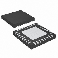
MAX3863ETJ+T Maxim Integrated Products, MAX3863ETJ+T Datasheet - Page 7

MAX3863ETJ+T
Manufacturer Part Number
MAX3863ETJ+T
Description
IC LASR DRVR 2.7GBPS 3.6V 32TQFN
Manufacturer
Maxim Integrated Products
Type
Laser Diode Driver (Fiber Optic)r
Datasheet
1.MAX3863ETJ.pdf
(15 pages)
Specifications of MAX3863ETJ+T
Data Rate
2.7Gbps
Number Of Channels
1
Voltage - Supply
3.15 V ~ 3.6 V
Current - Supply
58mA
Current - Modulation
80mA
Current - Bias
100mA
Operating Temperature
-40°C ~ 85°C
Package / Case
32-WFQFN Exposed Pad
Mounting Type
Surface Mount
Lead Free Status / RoHS Status
Lead free / RoHS Compliant
The MAX3863 laser driver has two main components: a
high-speed modulation driver and a biasing block with
APC. The clock and data inputs to the modulation driver
use CML logic levels. The optional clock signal synchro-
nizes data transitions for minimum pattern-dependent jit-
ter. Outputs to the laser diode consist of a switched
modulation current and a steady bias current. The APC
loop adjusts the laser diode bias current to maintain con-
stant average optical power. Compensation of the modu-
lation current can be programmed to keep a constant
extinction ratio over time and temperature. The modula-
tion output stage uses a programmable current source
with a maximum current of 80mA. A high-speed differen-
tial pair switches the source to the laser diode. The rise
and fall times are typically 50ps.
To eliminate pattern-dependent jitter in the input data, a
synchronous differential clock signal should be con-
nected to the CLK+ and CLK- inputs, and the RTEN
control input should be connected low. The input data
is retimed on the rising edge of CLK+. If RTEN is tied
high or is left floating, the retiming function is disabled,
and the input data is directly connected to the output
stage. Leave CLK+ and CLK- open when retiming is
disabled.
Figure 1. AC Characterization
Optional Input Data Retiming
_______________________________________________________________________________________
DATA+
DATA-
CLK+
CLK-
Detailed Description
2.7Gbps Laser Driver with Modulation
50Ω
50Ω
50Ω
V
50Ω
CC
V
DATA+
DATA-
CLK+
CLK-
CC
RTEN
MAX3863
V
V
CC
CC
APCFILT1
EN
MODN
MOD
BIAS
The MK+ and MK- outputs monitor the input signal
mark density. With a 50% mark density, both outputs
are the same voltage. More ones cause the MK+ volt-
age to increase and the MK- voltage to decrease.
Fewer ones than zeros cause MK- to be at a higher
voltage than MK+.
A pulse-width adjustment range of 50% to 150%
(±185ps) is available at 2.7Gbps. This feature compen-
sates pulse-width distortion elsewhere in the system.
Resistors at the PWC+ and PWC- pins program the
pulse width. The sum of the resistors is 1kΩ. The pins
can be left open for a 100% pulse width. A voltage also
can control these pins. A differential voltage of 600mV
(typ) gives ±185ps of pulse-width distortion.
The MAX3863 incorporates an input to enable current
to the laser diode. When EN is low, the modulation and
bias outputs at the MOD pin are enabled. When EN is
high or floating, the output is disabled. In the disabled
condition, bias and modulation currents are off.
To prevent data errors caused by low supply, the
MAX3863 disables the laser diode current for supply
voltage less than 2.7V. The power-supply threshold and
15Ω
A
B
V
CC
V
CC
A
B
0.1μF
0.1μF
A - TOKO FSLB2520-330K
B - MURATA BLM11HA601SPT
25Ω
50Ω
Compensation
50Ω
Power-Supply Threshold
Mark-Density Outputs
OSCILLOSCOPE
Pulse-Width Control
50Ω
Output Enable
7


