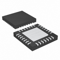
MAX3296CTI+T Maxim Integrated Products, MAX3296CTI+T Datasheet - Page 2

MAX3296CTI+T
Manufacturer Part Number
MAX3296CTI+T
Description
IC LASR DRVR 2.5GBPS 5.5V 28TQFN
Manufacturer
Maxim Integrated Products
Type
Laser Diode Driver (Fiber Optic)r
Datasheet
1.MAX3296CTI.pdf
(28 pages)
Specifications of MAX3296CTI+T
Data Rate
2.5Gbps
Number Of Channels
1
Voltage - Supply
3 V ~ 5.5 V
Current - Supply
52mA
Current - Modulation
30mA
Operating Temperature
0°C ~ 70°C
Package / Case
28-WFQFN Exposed Pad
Mounting Type
Surface Mount
Lead Free Status / RoHS Status
Lead free / RoHS Compliant
ABSOLUTE MAXIMUM RATINGS
Supply Voltage at V
Voltage at
Voltage at OUT+, OUT- .........................(V
Current into FAULT, FAULT, POR, SHDNDRV....-1mA to +25mA
Current into OUT+, OUT- ....................................................60mA
Continuous Power Dissipation (T
ELECTRICAL CHARACTERISTICS
(V
see Figure 1a.)
3.0V to 5.5V, 1.25Gbps/2.5Gbps
LAN Laser Drivers
Stresses beyond those listed under “Absolute Maximum Ratings” may cause permanent damage to the device. These are stress ratings only, and functional
operation of the device at these or any other conditions beyond those indicated in the operational sections of the specifications is not implied. Exposure to
absolute maximum rating conditions for extended periods may affect device reliability.
2
Supply Current
Data Input Voltage Swing
TTL Input Current
TTL Input High Voltage
TTL Input Low Voltage
FAULT, FAULT Output High
Voltage
FAULT, FAULT Output Low
Voltage
BIAS GENERATOR (Note 1)
BIASDRV Current, Shutdown
BIASDRV Current Sink
BIASDRV Current Source
REF Voltage
MD Nominal Voltage
MD Voltage During Fault
MD Input Current
MON Input Current
POWER-ON RESET
POR Threshold
POR Hysteresis
FAULT DETECTION
REF Fault Threshold
MD High Fault Threshold
MD Low Fault Threshold
MON Fault Threshold
MODSET, TC Fault Threshold
32-Pin TQFP (derate 14.3mW/°C above +70°C).........1100mW
CC
REF, POL, POL, MD, MON, BIASDRV,
MODSET, TC.......................................................-0.5V to (V
_______________________________________________________________________________________
= +3.0V to +5.5V, T
PARAMETER
EN, EN, PORDLY, FLTDLY, LV, IN+, IN-,
CC
..........................................-0.5V to +7.0V
A
= 0°C to +70°C, unless otherwise noted. Typical values are at V
A
= +70°C)
SYMBOL
V
V
V
I
V
V
V
CC
MD
OH
OL
ID
IH
IL
CC
- 2V) to (V
Figure 1a, R
Total differential signal, peak-to-peak, Figure 1a
0
I
I
EN = GND
FAULT = low, V
FAULT = low, V
I
APC loop is closed
Common-cathode configuration
Common-anode configuration
Normal operation (FAULT = low)
V
LV = GND
LV = open
MAX3286/MAX3288/MAX3296/MAX3298
OH
OL
REF
MON
V
= 1mA
= -100µA
PIN
CC
= V
2mA, MON = V
CC
+ 0.5V)
CC
+ 2V)
V
CC
MOD
BIASDRV
BIASDRV
CONDITIONS
= 1.82k
CC
Operating Temperature Range...............................0°C to +70°C
Operating Junction Temperature Range ..............0°C to +150°C
Processing Temperature (die) .........................................+400°C
Storage Temperature Range .............................-55°C to +150°C
Lead Temperature (soldering, 10s) .................................+300°C
28-Pin QFN and 28-Pin Thin QFN
(derate 28.7mW/°C above +70°C) ..............................2300mW
16-Pin TSSOP (derate 27mW/°C above +70°C) .........2162mW
0.6V
V
CC
- 1V
CC
= +3.3V, R
V
V
MD
MD
V
-100
2.45
1.55
2.65
MIN
200
600
2.4
0.8
0.8
3.9
CC
-1
-2
2
2
+ 5%
- 20%
-
V
TC
CC
+0.16
TYP
2.65
0.44
150
1.7
0.4
52
= open and T
- 0.8
V
MD
V
MD
+ 20%
+100
V
MAX
1660
2.85
1.85
3.00
2.95
480
0.8
0.4
1.2
4.5
0.9
+1
+2
CC -
75
- 5%
6
A
= +25°C;
UNITS
mV
mA
mA
mA
mV
mV
µA
µA
µA
µA
V
V
V
V
V
V
V
V
V
V


