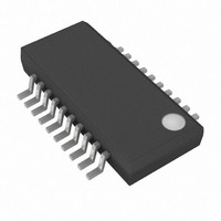
MAX3766EEP Maxim Integrated Products, MAX3766EEP Datasheet - Page 15

MAX3766EEP
Manufacturer Part Number
MAX3766EEP
Description
IC LASR DRVR 622MBPS 5.5V 20QSOP
Manufacturer
Maxim Integrated Products
Type
Laser Diode Driver (Fiber Optic)r
Datasheet
1.MAX3766EEP.pdf
(20 pages)
Specifications of MAX3766EEP
Data Rate
622Mbps
Number Of Channels
1
Voltage - Supply
4.5 V ~ 5.5 V
Current - Supply
25mA
Current - Modulation
60mA
Current - Bias
80mA
Operating Temperature
-40°C ~ 85°C
Package / Case
20-QSOP
Mounting Type
Surface Mount
Operating Supply Voltage
5 V
Supply Current
25 mA
Maximum Operating Temperature
+ 85 C
Maximum Power Dissipation
590 mW
Minimum Operating Temperature
- 40 C
Mounting Style
SMD/SMT
Lead Free Status / RoHS Status
Contains lead / RoHS non-compliant
Available stocks
Company
Part Number
Manufacturer
Quantity
Price
Company:
Part Number:
MAX3766EEP
Manufacturer:
MAXIM
Quantity:
20
Part Number:
MAX3766EEP
Manufacturer:
MAXIM/美信
Quantity:
20 000
Company:
Part Number:
MAX3766EEP+
Manufacturer:
Maxim
Quantity:
670
Company:
Part Number:
MAX3766EEP+
Manufacturer:
HITTITE
Quantity:
5 000
Part Number:
MAX3766EEP+
Manufacturer:
MAXIM/美信
Quantity:
20 000
Company:
Part Number:
MAX3766EEP+T
Manufacturer:
3M
Quantity:
230
The MAX3766 is a high-frequency product. The perfor-
mance of the circuit is largely dependent upon the lay-
out of the circuit board.
Use a multilayer circuit board with a dedicated ground
plane. Use short laser package leads placed close to
OUT+ and OUT- to keep output inductance low. Power
supplies should be capacitively bypassed to the
ground plane with surface-mount capacitors placed
near the power-supply pins.
1) Laser output is ringing and contains overshoot.
Figure 9. Input Terminations
Automatic Power Control and Safety Shutdown
SINGLE-ENDED TERMINATION IS SHOWN. THE OTHER INPUT SHOULD BE
TERMINATED SIMILARLY, OR CONNECTED TO V
This is often caused by inductive laser packaging.
Try reducing the lead length of the laser pins. Modify
the compensation network to reduce the driver’s out-
put edge speed (see Design Procedure). This prob-
lem can also occur if the voltage at OUT+, OUT-, or
BIAS is below V
supply voltage, or reducing the modulation current.
CMOS OUTPUT
PECL OUTPUT
RF OR NON-
OUTPUT
TTL OR
PECL
Solutions to Common Problems
______________________________________________________________________________________
CC
10kΩ
R1
- 2.5V. Test this by increasing the
V
CC
- 2V
Layout Considerations
622Mbps LAN/WAN Laser Driver with
50Ω
180Ω
R3
11.8k
V
V
CC
CC
CC
- 1.3V.
68Ω
R2
2.87k
IN
IN
IN
MAX3766
MAX3766
MAX3766
2) Low-frequency oscillation on the bias-current
3) Modulation driver is not needed.
4) APC is not needed.
5) Laser edge switching speed is low.
The MAX3766 uses bondpads with gold metalization.
Make connections to the die with gold wire only, using
ball bonding techniques. Wedge bonding is not recom-
mended. Pad size is 4 mils (0.1mm) square. Die thick-
ness is typically 15 mils (0.38mm).
Figure 11 shows typical models for the inputs and out-
puts of the MAX3766, including package parasitics. If
dice are used, replace the package parasitic elements
with bondwire parasitic elements.
Figure 10. External Laser Shutdown Circuit
FAIL
Ensure C
If only the bias-current driver and safety circuits are
needed, connect IN+ to V
nected. Connect OUT+ and OUT- to the supply.
Leave MOD, TC, and REF2 unconnected.
If only the high-speed modulation driver is used,
connect BIAS to V
FAIL, and BIASMAX unconnected. Connect SAFETY
to ground.
Refer to the Design Bias Filter section. It may be
necessary to select L
ing frequency.
output.
V
CC
5.1k
MD
100k
≥ 0.1µF.
CC
5.1k
BIAS
, and leave POWERSET, MD,
V
CC
RESET
with a higher self-resonat-
CC
, and leave IN- uncon-
Wire Bonding Die
Interface Models
FAIL
MAX3766
OUT+
V
CC
LASER
15


