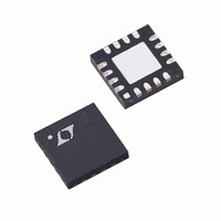
LTC5100EUF#TRPBF Linear Technology, LTC5100EUF#TRPBF Datasheet - Page 11

LTC5100EUF#TRPBF
Manufacturer Part Number
LTC5100EUF#TRPBF
Description
IC DRIVER VCSEL 3.2GBPS 16QFN
Manufacturer
Linear Technology
Type
Laser Diode Driverr
Datasheet
1.LTC5100EUF.pdf
(52 pages)
Specifications of LTC5100EUF#TRPBF
Data Rate
3.2Gbps
Number Of Channels
1
Voltage - Supply
3.135 V ~ 3.465 V
Current - Supply
54mA
Current - Modulation
12mA
Operating Temperature
-40°C ~ 85°C
Package / Case
16-QFN
Mounting Type
Surface Mount
Lead Free Status / RoHS Status
Lead free / RoHS Compliant
Available stocks
Company
Part Number
Manufacturer
Quantity
Price
PI FU CTIO S
V
High Speed Circuitry. These pins are internally connected.
Connect Pins 1, 4, 9 and 12 to the ground plane with
minimal trace lengths. Place a minimum of four vias
(preferably nine vias) to the ground plane in the Exposed
Pad area. Most of the high speed modulation current is
returned through the Exposed Pad (Pin 17).
IN
The inputs are differential with internal termination resis-
tors. The input amplifier is internally AC coupled. With
current mode logic (CML) enabled, the inputs are indepen-
dently terminated to V
CML disabled, the inputs provide 100 differential termi-
nation and permit rail-to-rail common mode range. The
input pins can be AC coupled with external capacitors.
When externally AC coupled, the input pins self-bias to
V
FAULT (Pin 5): Signals One of Five Safety Fault Con-
ditions: laser overcurrent, overpower, underpower, power
supply undervoltage and memory load error. The pin can
be programmed active high or active low with the
Flt_pin_polarity bit. The FAULT pin can be programmed to
four different drive modes with the Flt_drv_mode bits.
SDA, SCL (Pins 6, 7): Serial Interface Data and Clock
Signals. The pins are open drain with a 100 A internal pull-
up current. An external pull-up resistor can be added to
drive larger capacitive loads.
V
Modulation Circuitry. Filter this pin with a ferrite bead and
bypass the pin directly to the ground plane with a 10nF
ceramic capacitor.
SS
DD(HS)
DD(HS)
+
U
, IN
(Pins 1, 4, 9, 12, 17): Ground for Digital, Analog and
–
/2. The Cml_en bit selects the termination mode.
(Pins 2, 3): High Speed Laser Modulation Inputs.
(Pin 8): Power Input for the High Speed Laser
U
U
DD(HS)
with 50
resistors. With
MODA, MODB (Pins 11, 10): High Speed Laser Modula-
tion Outputs. MODA and MODB are connected on-chip
and driven by an open-drain output transistor. One of
these pins should be connected to the laser. The other
should be connected to a termination resistor. See the
Applications Information section for details.
MD (Pin 13): Monitor Diode Input for Automatic Power
Control of the Laser Bias Current. The MD pin allows
connection to the cathode or anode of the monitor diode.
The Md_polarity bit selects the polarity of the monitor
diode.
SRC (Pin 14): Current Source for Biasing the Laser. See
the Applications Information section for details.
EN (Pin 15): Transmitter Enable and Disable Input. This
input is TTL compatible and can be programmed for active
high or active low operation with the En_polarity bit. An
internal 10 A current source disables the transmitter if the
EN pin becomes disconnected. This safety feature oper-
ates whether the EN pin is active high or active low.
V
Analog Circuitry. Connect this pin to V
a short trace. No bypassing is needed at the V
trace length to the V
10mm long.
DD
(Pin 16): Power Input for Digital and Low Speed
DD(HS)
bypass capacitor is less than
DD(HS)
LTC5100
(Pin 8) with
DD
sn5100 5100fs
pin if the
11


