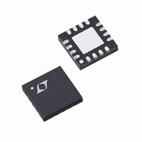
LTC5100EUF#TR Linear Technology, LTC5100EUF#TR Datasheet - Page 49

LTC5100EUF#TR
Manufacturer Part Number
LTC5100EUF#TR
Description
IC DRIVER VCSEL 3.2GBPS 16QFN
Manufacturer
Linear Technology
Type
Laser Diode Driverr
Datasheet
1.LTC5100EUF.pdf
(52 pages)
Specifications of LTC5100EUF#TR
Data Rate
3.2Gbps
Number Of Channels
1
Voltage - Supply
3.135 V ~ 3.465 V
Current - Supply
54mA
Current - Modulation
12mA
Operating Temperature
-40°C ~ 85°C
Package / Case
16-QFN
Mounting Type
Surface Mount
Lead Free Status / RoHS Status
Contains lead / RoHS non-compliant
Lead Free Status / RoHS Status
Contains lead / RoHS non-compliant
Available stocks
Company
Part Number
Manufacturer
Quantity
Price
APPLICATIO S I FOR ATIO
Figure 31 and Figure 32 show the schematic and layout of
a minimum reflection coefficient, minimum peaking solu-
tion. Two capacitors, C1 and C2 are used to further reduce
the inductance in the termination network. C2 has two vias
to the ground plane.
TEMPERATURE COMPENSATION
The LTC5100 has first and second order digital tempera-
ture compensation for the laser bias current, laser modu-
lation current, and monitor diode current. Recall that in
constant current control mode, the LTC5100 provides
direct temperature compensation of the laser bias current
and the laser modulation current. In automatic power
control mode, the laser bias current is under closed-loop
control and the LTC5100 provides temperature compen-
sation for the monitor diode current and the laser modu-
lation current. The simplest procedure for determining the
temperature coefficients (TC1 and TC2 in Equation 12,
Equation 18, Equation 23, and Equation 29) is as follows:
• Select a nominal or representative laser diode and
• Set all temperature coefficients to zero.
• Place the transceiver module in a temperature chamber
• Record the LTC5100’s temperature reading, T_int, at
• Select a convenient value for T_nom, the nominal tem-
• Find the best values of TC1 and TC2 by fitting the
To configure the LTC5100 for normal operation, set the
nominal current to the value found at the nominal tem-
perature. Set TC1 and TC2 to the values determined by the
best fit of the data. For standalone operation, store these
values in the EEPROM. For microprocessor operation,
store the values in the microprocessor’s internal non-
volatile memory or in another source of nonvolatile memory
and load them into the LTC5100 after power-up.
assemble it into a transceiver module with the LTC5100.
and find the values of Ib_nom, Im_nom, and Imd_nom
that give constant average optical power and extinction
ratio at several temperature points.
each temperature point.
perature. (It is customary, but not mandatory, to use
25 C for the nominal temperature.)
quadratic temperature compensation formula (Equa-
tion 12) to the experimental values of Ib_nom, Im_nom,
Imd_nom, and T_int.
U
U
W
U
The above procedure not only corrects for the laser
temperature drift, but also corrects the small temperature
drift found in the LTC5100’s internal references.
DEMONSTRATION BOARD
Figure 33 shows the schematic of the DC499 demonstra-
tion board. Details of the use of this demo board and
accompanying software can be found in the DC499 demo
board manual. Figure 34 shows the layout of the demo
board and Table 31 gives the bill of materials for the demo
board.
The core applications circuit for the LTC5100 VCSEL
driver appears inside the box in Figure 33. This is the
complete circuit for an optical transceiver module, includ-
ing power supply filtering. It consists of the LTC5100 with
EEPROM for storing setup parameters, L1 and C3 for
power supply filtering, and R1, C1, and C2 for terminating
the 50 modulation output. The circuitry outside the box
in Figure 33 is for support of the demonstration. 5V power
enters through 2-pin connector P2 and is regulated by U3
to 3.3V to power the LTC5100. Connector P1 sends 5V
power and serial control signals to another board, allow-
ing a personal computer to control the LTC5100. U4
produces 1.8VDC to bias the modulation output for elec-
trical eye measurements.
High speed data enters the LTC5100 through SMA con-
nectors J1 and J2. The LTC5100 high speed inputs are
internally AC coupled with rail-to-rail common mode input
voltage range. The input signal swing can go as much as
300mV above V
mance or causing excessive current flow. The high speed
inputs may be AC coupled, in which case the common
mode voltage floats to mid-supply or 1.65V nominally.
A common cathode VCSEL can be attached to the demo
board via SMA connector J3. R1 establishes a precision,
low reflection coefficient 50 modulation drive. By main-
taining a wide band microwave quality 50
length of the connection to the laser can be arbitrarily long.
The LTC5100 generates 20% to 80% transition times of
60ps (80ps 10% to 90%), corresponding to an instanta-
neous transition filtered by a 4.4GHz Gaussian lowpass
filter. At these speeds the primary limitation on line length
is high frequency loss. For high grade, low loss laboratory
cabling with silver coated center conductor and foamed
PTFE dielectric, a practical limit is about 30cm.
DD
or below V
SS
without degrading perfor-
LTC5100
path, the
sn5100 5100fs
49


