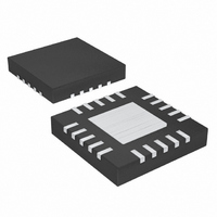
MAX3643ETG+ Maxim Integrated Products, MAX3643ETG+ Datasheet - Page 10

MAX3643ETG+
Manufacturer Part Number
MAX3643ETG+
Description
IC LASR DRVR 2.5GBPS 3.6V 24TQFN
Manufacturer
Maxim Integrated Products
Type
Laser Diode Driver (Fiber Optic)r
Datasheet
1.MAX3643ETG.pdf
(15 pages)
Specifications of MAX3643ETG+
Data Rate
2.5Gbps
Number Of Channels
1
Voltage - Supply
3 V ~ 3.6 V
Current - Supply
32mA
Current - Modulation
85mA
Current - Bias
70mA
Operating Temperature
-40°C ~ 85°C
Package / Case
24-TQFN Exposed Pad
Mounting Type
Surface Mount
Lead Free Status / RoHS Status
Lead free / RoHS Compliant
155Mbps to 2.5Gbps Burst-Mode Laser Driver
The MAX3643 laser driver includes a bias current gen-
erator, bias current monitor, modulation current genera-
tor, laser drive outputs, and monitor diode sample and
hold. LVPECL-compatible inputs are provided for both
high-speed data and burst enable. The high-speed
burst-enable input signal is replicated on an LVCMOS
output for use by the controller.
Laser diode modulation current amplitude is controlled
by the current out of the MODSET pin, and bias current
by the current out of the BIASSET pin, according to:
A voltage source and two op amps are provided to
enable I
resistor to ground or a current digital-to-analog convert-
er (DAC). The high-impedance op amp reference input
can be externally controlled, so that the modulation and
bias currents can also be set using voltage DACs.
Typical laser diodes have an absolute maximum rating
of 150mA. To reduce the possibility of laser damage,
the modulation current and bias current are shut off if
the sum I
by R
The laser diode bias current can be monitored by measur-
ing the voltage across an external load resistor connected
from BCMON to ground. For example, a 1kΩ resistor from
BCMON to ground gives the following relationship:
The voltage at BCMON must be below 1.4V for proper
operation.
The modulation current ranges from 10mA to 85mA, as
set by the current through MODSET. The laser modula-
tion current output OUT+ is optimized to drive a 15Ω
load, and must be DC-coupled. A series damping resis-
tor, R
diode. The combined value of the series damping resis-
tor and the laser diode equivalent series resistance
10
IMAX
______________________________________________________________________________________
D
, provides impedance matching to the laser
MODSET
; see the Typical Operating Characteristics .
MOD
V
BCMON
+ I
I
I
and I
MOD
BIAS
BIAS
Laser Diode Modulation and
Laser Diode Modulation and
=
I
Detailed Description
BIASSET
BIAS
= I
= I
attempts to exceed the limit set
Bias Current Generators
MODSET
BIASSET
×
Bias Current Monitor
Bias Current Limiter
G
BSM
to be set using either a
x 88
x 88
× 1 Ω
Output Drivers
k
should be close to 15Ω. An RC shunt compensation
network, R
diode cathode and ground should also be provided to
reduce optical output aberrations and duty-cycle dis-
tortion caused by laser diode parasitic inductance. The
values of R
the laser diode and PCB layout characteristics for opti-
mal optical eye performance (refer to Application
Note 274: HFAN-02.0: Interfacing Maxim Laser Drivers
with Laser Diodes ). The OUT- pin is connected through
a 15Ω resistor and switching diode to the laser diode
anode. The switching diode at OUT- improves the opti-
cal output eye and burst-enable delay by better match-
ing the laser diode characteristics.
For data rates greater than 1Gbps, a parallel RL peak-
ing network, R
anode and V
a differential drive for the laser diode to improve rise/fall
times and reduce jitter. The values of R
also adjusted to match the laser diode and PCB layout
characteristics for optimal optical eye performance.
The bias current ranges from 1mA to 70mA, as set by
the current through BIASSET. Current in the BIAS out-
put switches at high speed when bursting; therefore,
the BIAS+ pin should be connected directly through a
resistor, equal to R
cathode. The BIAS- pin is connected through a 10Ω
resistor and switching diode to V
When the BEN input is high, the laser driver sinks bias
and modulation current according to the settings at
MODSET and BIASSET. When the BEN input is low, the
BIAS+ and OUT+ currents both shut off within 2ns.
Note that when BEN is low, the bias current is shunted
through the BIAS- output and the modulation current
through the OUT- output.
Laser monitor diode current is only generated when
there is an optical output (BEN is active). When BEN is
inactive, the monitor current is zero, reflecting the fact
that the laser is off. A sample-and-hold circuit, trig-
gered by the state of the BEN input, is provided in the
MAX3643. During the burst-enable active period, the
voltage present at MDIN is stored on an internal sam-
ple-and-hold capacitor; and during the burst-enable
inactive period, that voltage is output on MDOUT; see
the timing diagram in Figure 2.
While the internal sample-and-hold is sampling (BEN
active), MDOUT voltage takes a 1.2V reference level.
COMP
COMP
CC
P
Monitor Diode Sample and Hold
/L
is recommended. This network creates
/C
P
and C
, connected between the laser diode
COMP
D
as determined above, to the laser
COMP
, connected between the laser
can be adjusted to match
CC
.
P
and L
P
are


