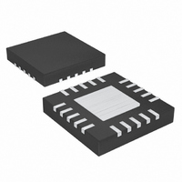
MAX3795ETG+ Maxim Integrated Products, MAX3795ETG+ Datasheet - Page 8

MAX3795ETG+
Manufacturer Part Number
MAX3795ETG+
Description
IC DRIVER VCSEL W/MON 24-TQFN
Manufacturer
Maxim Integrated Products
Type
Laser Diode Driverr
Datasheet
1.MAX3795ETG.pdf
(15 pages)
Specifications of MAX3795ETG+
Data Rate
4.25Gbps
Number Of Channels
1
Voltage - Supply
2.97 V ~ 3.63 V
Current - Supply
71mA
Current - Modulation
15mA
Current - Bias
15mA
Operating Temperature
-40°C ~ 85°C
Package / Case
24-TQFN Exposed Pad
Mounting Type
Surface Mount
Operating Supply Voltage
3.3 V
Minimum Operating Temperature
- 40 C
Mounting Style
SMD/SMT
Lead Free Status / RoHS Status
Lead free / RoHS Compliant
1Gbps to 4.25Gbps Multirate VCSEL Driver
with Diagnostic Monitors
8
1, 10, 13
7, 16, 20
_______________________________________________________________________________________
PIN
EP
11
12
14
15
17
18
19
21
22
23
24
2
3
4
5
6
8
9
Exposed Pad
TX_DISABLE
SQUELCH
BIASMON
PWRMON
PEAKSET
MODSET
BIASSET
FAULT
NAME
COMP
OUT+
OUT-
GND
BIAS
V
TC1
TC2
REF
IN+
MD
IN-
CC
Ground
Transmit Disable. Driver output is disabled when TX_DISABLE is high or left unconnected. The
driver output is enabled when the pin is asserted low.
Noninverted Data Input
Inverted Data Input
Fault Indicator. Open-drain output with ESD protection. FAULT is asserted high during a
fault condition.
Squelch Enable. Squelch is enabled when the pin is set high. Squelch is disabled when the pin is
set low or left open.
+3.3V Supply Voltage
Temperature Compensation Set Pin 1. A resistor placed between TC1 and TC2 (R
temperature coefficient of the laser modulation current.
Temperature Compensation Set Pin 2. A resistor placed between TC1 and TC2 (R
temperature coefficient of the laser modulation current.
Modulation Set. A resistor connected from MODSET to ground (R
modulation current amplitude.
Peaking Current Set. A resistor connected between PEAKSET and ground (R
peaking current amplitude. To disable peaking, leave PEAKSET open.
Inverted Modulation Current Output
Noninverted Modulation Current Output
Bias-Current Set. When a closed-loop configuration is used, connect a 1.7kΩ resistor between
ground and BIASSET to program the maximum bias current. When an open configuration is used,
connect a resistor between BIASSET and ground (R
Bias-Current Output
Bias-Current Monitor. The output of BIASMON is a sourced current proportional to the bias current.
A resistor connected between BIASMON and ground (R
referenced bias monitor.
Compensation Pin. A capacitor between COMP and MD compensates the APC. A typical value of
0.047µF is recommended. For open-loop configuration, short the COMP pin to GND to deactivate
the APC circuit.
Monitor Diode Connection
Refer ence P i n. Refer ence m oni tor used for AP C . A r esi stor b etw een RE F and M D ( R
the p hotom oni tor cur r ent w hen the AP C l oop i s cl osed .
Average Power Monitor. The pin is used to monitor the transmit optical power. For open-loop
configuration, connect PWRMON to GND.
Ground. Must be soldered to the circuit board ground for proper thermal and electrical
performance. See the Layout Considerations section.
FUNCTION
BIASSET
BIASMON
) to program the VCSEL bias current.
) can be used to form a ground-
MODSET
) programs the desired
Pin Description
PEAKSET
P WRS E T
TC
TC
) programs the
) programs the
) programs the
) p r og r am s


