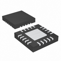
MAX3740AETG+ Maxim Integrated Products, MAX3740AETG+ Datasheet - Page 12

MAX3740AETG+
Manufacturer Part Number
MAX3740AETG+
Description
IC DRIVER SFP VCSEL 24-TQFN
Manufacturer
Maxim Integrated Products
Type
Laser Diode Driverr
Datasheet
1.MAX3740AETG.pdf
(15 pages)
Specifications of MAX3740AETG+
Data Rate
3.2Gbps
Number Of Channels
1
Voltage - Supply
2.97 V ~ 3.63 V
Current - Supply
55mA
Current - Modulation
15mA
Current - Bias
15mA
Operating Temperature
-40°C ~ 85°C
Package / Case
24-TQFN Exposed Pad
Mounting Type
Surface Mount
Package
24TQFN EP
Maximum Data Rate
3.2 Gbps
Transmission Media Type
Optical Fiber
Power Supply Type
Analog
Typical Supply Current
55 mA
Maximum Operating Supply Voltage
6 V
Lead Free Status / RoHS Status
Lead free / RoHS Compliant
3.2Gbps SFP VCSEL Driver with Diagnostic
Monitors
The modulation current output of the MAX3740A is con-
trolled by a resistor (R
MODSET and ground. The R
the amount of current being sourced to the VCSEL. The
modulation current is given by the following:
It is important to note that the modulation current being
sourced by the MAX3740A is affected by the load
impedance of the VCSEL. The Modulation Current vs.
R
shows the current into a 50Ω electrical load.
The bias current output of the MAX3740A is controlled
by a resistor (R
ground. In open-loop operation the R
the bias current level of the VCSEL. In closed-loop
operation the R
rent provided by the APC. The bias current is given by
the following:
The Bias Current vs. R
the Typical Operating Characteristics .
To ensure stable operation of the APC circuit, the time
constant of the MD node should be shorter than the
APC time constant. (t
For typical I
photodiode with capacitance less than 500pF.
Compute the required modulation tempco from the
slope efficiency of the laser at T
higher temperature. Then select the value of R
the Typical Operating Characteristics . For example,
suppose a laser has a slope efficiency (SE) of
12
I
I
MOD
MOD
MODSET
Programming Modulation-Current Tempco
___________________________________________________
=
=
t MD
[
⎡
⎢
⎢
⎣
(
⎛
⎜
⎝
I
MODSET
graph in the Typical Operating Characteristics
200
I
I
≤
BIAS
BIAS
t APC
Programming Modulation Current
PD
20
+
BIASSET
BIASSET
=
=
R
= 400µA, R
(
,
1
MODSET
⎛
⎜
⎝
I
)
BIASSET
200
×
R
MD
30
APC
Programming Bias Current
+
]
) placed between BIASSET and
BIASSET
controls the maximum bias cur-
×
×
R
1 2
= 5µs if C
C
⎞
⎟ ×
⎠
.
BIASSET
⎡
⎢
⎣
MODSET
)
R
MD
×
Photodiode Selection
PWRSET
OUT
30
34
MODSET
≤
R
⎤
⎥
⎥
⎦
graph is also shown in
+
5
×
OUT
20
μ
⎞
⎟ ×
⎠
A
+
⎡
⎢
⎣
APC
s
) placed between
R
R
= +25°C and at a
=
+
OUT
34
= 500Ω, select a
LOAD
250
BIASSET
resistor controls
= 0.047µF).
R
+
OUT
ns
+
⎤
⎥
⎦
R
+
LOAD
controls
TC
from
⎤
⎥
⎦
0.021mW/mA at +25°C, which reduces to 0.018mW/mA
at +85°C. The temperature coefficient is given by the
following:
From the Typical Operating Characteristics , the value
of R
modulation temperature compensation is not desired,
short TC1 and TC2.
Program the average optical power by adjusting
R
desired monitor current to be maintained over tempera-
ture and lifetime. See the Monitor Diode Current vs.
R
section, and select the value of R
sponds to the required current.
The MAX3740A data inputs are SFP MSA compatible.
On-chip 100Ω differential input impedance is provided
for optimal termination (Figure 4). Because of the on-chip
biasing network, the MAX3740A inputs self-bias to the
proper operating point to accommodate AC-coupling.
Figure 4. Simplified Input Structure
Laser tempco
PWRSET
PWRSET
IN+
IN-
TC
PACKAGE
, which offsets the tempco of the laser, is 9kΩ. If
MAX3740A
1nH
1nH
graph in the Typical Operating Characteristics
. To select the resistance, determine the
0.5pF
0.5pF
Input Termination Requirements
= −
=
SE
(
2380
SE
25
Programming the APC Loop
85
V
V
×
ppm C
CC
CC
−
(
85 25
SE
50Ω
50Ω
/
−
°
25
16kΩ
24kΩ
)
)
×
1 6
E
PWRSET
V
CC
that corre-


