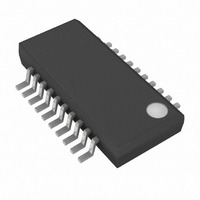
MAX3766EEP+ Maxim Integrated Products, MAX3766EEP+ Datasheet - Page 7

MAX3766EEP+
Manufacturer Part Number
MAX3766EEP+
Description
IC LASR DRVR 622MBPS 5.5V 20QSOP
Manufacturer
Maxim Integrated Products
Type
Laser Diode Driver (Fiber Optic)r
Datasheet
1.MAX3766EEP.pdf
(20 pages)
Specifications of MAX3766EEP+
Data Rate
622Mbps
Number Of Channels
1
Voltage - Supply
4.5 V ~ 5.5 V
Current - Supply
25mA
Current - Modulation
60mA
Current - Bias
80mA
Operating Temperature
-40°C ~ 85°C
Package / Case
20-QSOP
Mounting Type
Surface Mount
Operating Supply Voltage
5 V
Supply Current
25 mA
Maximum Operating Temperature
+ 85 C
Maximum Power Dissipation
590 mW
Minimum Operating Temperature
- 40 C
Mounting Style
SMD/SMT
Lead Free Status / RoHS Status
Lead free / RoHS Compliant
Figure 2 is a functional block diagram of the MAX3766
laser driver. The major functional blocks are the refer-
ence generator, PECL input buffer, laser-bias circuit,
modulation-current driver, automatic power control
(APC), failure detection, and safety circuit.
The MAX3766 provides adjustments for maximum
laser-bias current, laser modulation current, and aver-
age laser power. To program these adjustments, simply
use the currents obtained by inserting a resistor in
series with integrated voltage references REF1 and
REF2. The temperature coefficient (tempco) of REF1
compensates for the tempco of the bias, modulation,
and APC current mirrors. Therefore, a programming
current derived from REF1 is constant with tempera-
ture. REF2 provides a positive tempco, which can be
applied to the modulation current. A positive modula-
tion-current tempco will compensate for the thermal
characteristics of typical laser diodes. The modulation-
current tempco is programmed by an external resistor
(R
an internal 2kΩ resistor form a weighted sum of the
temperature-compensated reference (REF1) and the
temperature-increasing reference, which is buffered
and output at REF2. REF1 and REF2 are stable with no
bypass capacitance. Bypass filtering REF1 or REF2 is
not required.
Figure 1. Required Input Signal and Output Polarity
_______________Detailed Description
Automatic Power Control and Safety Shutdown
TC
V
IN+
), which is connected from REF1 to TC. R
VOLTS
- V
I
OUT+
V
V
V
V
IN+
IN+
IN-
IN-
IN-
DIFFERENTIAL INPUT
SINGLE-ENDED INPUT
RESULTING SIGNAL
_______________________________________________________________________________________
622Mbps LAN/WAN Laser Driver with
Reference Generator
TIME
500mV MIN
1800mV MAX
250mV MIN
900mV MAX
500mV MIN
1800mV MAX
I
MOD
TC
and
The differential PECL input signals are connected to the
high-speed PECL input buffer at IN+ and IN-. The input
impedance at IN+ and IN- is greater than 100kΩ, and
the input bias current is less than 10µA. The
MAX3766’s data inputs are not self-biasing. The com-
mon-mode input should be set by the external PECL
termination circuitry. To obtain good AC performance,
inputs should always be greater than 2.2V and less
than V
The laser modulation-current driver consists of a cur-
rent mirror and an emitter coupled pair. The mirror has
a gain of +30mA/mA. Modulation-current amplitude is
programmed with external resistor R
from REF2 to MOD. R
with R
The MAX3766 AC output drives up to 60mA of laser
current. Pulse-width distortion and overshoot are lowest
between 30mA and 60mA. However, output edge
speed increases at lower currents. When the output
current is between 2mA and 60mA, the edge speed is
suitable for communications up to 622Mbps. Edge
speeds below 30mA are suitable for communications up
to 1.25Gbps (see Typical Operating Characteristics).
The modulation-current tempco can be programmed
with an external resistor R
Reference Generator section. An internal 520Ω resistor
is included to limit the maximum modulation current if
MOD is connected directly to REF2.
If the MAX3766 is shut down or disabled, the modula-
tion programming current is shunted to ground. Any
remaining modulation current is switched to OUT-.
For optimum performance, the voltage at OUT+ and
OUT- must always exceed V
The laser bias circuit is a current mirror with a gain of
+40mA/mA. Redundant controls disable the bias current
during a shutdown or disable event: the programming
current is switched off, and any remaining bias output
current is switched away from the laser. Ensure that the
voltage at BIAS always remains above V
bias circuit is not used, connect BIAS to V
TC
CC
.
= 0Ω.
R
Laser Modulation-Current Driver
MOD
=
MOD
1.55V 30
I
can be estimated as follows:
MOD
CC
( )
TC
- 2.5V.
, as described in the
Laser Bias Circuit
PECL Input Buffer
− 520Ω
MOD
CC
CC
- 2.5V. If the
.
connected
7


