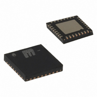
SY88236LMG TR Micrel Inc, SY88236LMG TR Datasheet - Page 15

SY88236LMG TR
Manufacturer Part Number
SY88236LMG TR
Description
IC LASER DVR BURST 2.5GBPS 32MLF
Manufacturer
Micrel Inc
Type
Laser Diode Driver, Burst Moder
Datasheet
1.SY88236LMG.pdf
(19 pages)
Specifications of SY88236LMG TR
Data Rate
2.5Gbps
Number Of Channels
2
Voltage - Supply
3 V ~ 3.6 V
Current - Supply
90mA
Current - Modulation
85mA
Current - Bias
70mA
Operating Temperature
-40°C ~ 85°C
Package / Case
32-MLF®, QFN
Mounting Type
Surface Mount
Lead Free Status / RoHS Status
Lead free / RoHS Compliant
Other names
576-3730-2
Functional Description
Laser Driver
The laser driver is comprised from a modulator, a bias
circuit, and a digital APC loop.
The driver features bias and modulation current
monitoring functions, which can be configured for optical
power monitoring.
BIAS and Modulation Setting
Bias and modulation currents are set by installing
resistors from APCSET to ground and from MODSET to
ground respectively or by applying a negative current at
those pins. I
I
and I
BIASMAX
A resistor between BIASMAX pin and ground sets the
maximum bias the driver can sink. At normal operation,
the bias current tracks the laser optical power through
the laser monitoring photodiode and the APC loop to
compensate for any power deviation from the nominal
value set at the start of operation using APCSET. If for
any failure (laser or photodiode degradation, open
feedback circuit, etc.) the APC loop keeps increasing the
bias current to compensate for the low power indication,
the bias current will stop increasing when it reaches
BIASMAX value and continues to operate at that
maximum value and APCFAULT is asserted.
BIASMAX also sets the bias current when the circuit is
operating in the open loop mode.
APC Loop Function
At start up, with the driver enabled, TXDIS low and
BEN+
microseconds and its back facet monitoring photodiode
starts to generate a photocurrent proportional to the
optical power. The photocurrent is fed back to the MD
pin on the driver where it’s converted to a voltage. The
conversion voltage is compared to APCSET on the
driver. At equilibrium, the feedback voltage equals the
APCSET voltage and the laser optical power reaches its
nominal value. If the laser power deviates from its
nominal value, the APC loop brings it back to its nominal
setting.
APC Loop Failure
The APCFAULT is asserted Low if the bias current
reaches BIASMAX or if the APC loop counter reaches its
minimum or its maximum counts.
Interfacing the Driver with the Laser Diode
As shown on the “Typical Application” drawing, MOD+
pin is connected to the laser cathode through a 10
BIASMAXSET
Micrel, Inc.
June 2009
MODSET
high,
, and I
are shown on page 10.
BIAS
the
variation versus R
MOD
laser
variation versus R
turns
BIASMAXSET
ON
within
MODSET
resistor and
resistor
a
Ω
few
15
resistor and MOD- pin is connected to VCC with a 15 Ω
resistor equivalent to 10 Ω (damping resistor) in series
with the laser (equivalent resistor of 5 Ω). The laser can
be driven differentially by connecting MOD- to the anode
of the laser through 15
isolating the anode of the laser from VCC with an
inductor.
Post Amplifier
The post amplifier detects and amplifies signals with
data rates from DC up to 3.2Gbps, and amplitude as
small as 5mV
post amplifier when the input signal is absent or lower
than the minimum detectable level set by LOS
pin is provided, which can be connected to LOS/SD
output to turn off the output buffer when LOSS/SD is
asserted.
Input Amplifier/Buffer
Figure 1-d shows a simplified schematic of the input
stage. The high-sensitivity of the input amplifier allows
signals as small as 5mV
The input amplifier allows input signals as large as
1800mV
are linearly amplified with a typically 38dB differential
voltage gain. For input signals larger than 12mV
output signal is limited to typically 800mV
Output Buffer
The post amplifier CML output buffer is designed to drive
50Ω lines and is internally terminated with 50Ω to V
Figure 1e shows a simplified schematic of the output
stage.
Loss-of-Signal
The post amplifier generates a selectable chatter-free
loss-of-signal (LOS) or signal detect (SD) open-collector
TTL output as shown in Figure 2g. LOS/SD is used to
determine that the input amplitude is too small to be
considered as a valid input. When the LOSS function is
selected (LOS/SD_SEL=1), LOS/SD asserts high if the
input amplitude falls below the threshold set by LOSLVL
and de-asserts low otherwise. IF SD function is selected
(LOS/SD_SEL=0), LOS/SD asserts low if the input
amplitude falls below the threshold set by LOSLVL and
de-asserts high otherwise. LOS/SD can be fed back to
the JAM input to maintain output stability under a loss of
signal condition. Jam de-asserts low the true output
signal without removing the input signals. Typically, 3dB
LOS hysteresis is provided to prevent chattering.
Loss/Signal Detect Selection
A pin (LOS/SD_SEL) is provided to select between LOS
(set to high) or SD (set to low) function. It also controls
the internal circuitry of JAM input to follow LOS/SD
selection.
PP
. Small input signals below typically 12mV
PP
. To reduce the noise at the output of the
hbwhelp@micrel.com
Ω (15Ω pull
PP
to be detected and amplified.
-up removed) and
or (408) 955-1690
M9999-063009-A
PP
SY88236L/AL
.
LVL
, a JAM
PP
, the
CC
PP
.


