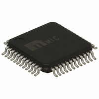
MIC2590B-2BTQ Micrel Inc, MIC2590B-2BTQ Datasheet - Page 11

MIC2590B-2BTQ
Manufacturer Part Number
MIC2590B-2BTQ
Description
IC PCI HOT PLUG CTLR DUAL 48TQFP
Manufacturer
Micrel Inc
Type
Hot-Swap Controllerr
Datasheet
1.MIC2590B-2YTQ.pdf
(23 pages)
Specifications of MIC2590B-2BTQ
Applications
PCI, PCI-X
Internal Switch(s)
No
Voltage - Supply
3.3V, 5V, ±12V
Operating Temperature
0°C ~ 70°C
Mounting Type
Surface Mount
Package / Case
48-TQFP
Lead Free Status / RoHS Status
Contains lead / RoHS non-compliant
Available stocks
Company
Part Number
Manufacturer
Quantity
Price
Part Number:
MIC2590B-2BTQ
Manufacturer:
MICREL/麦瑞
Quantity:
20 000
Part Number:
MIC2590B-2BTQTR
Manufacturer:
MICREL/麦瑞
Quantity:
20 000
Functional Description
Hot Swap Insertion
When circuit boards are inserted into systems carrying
live supply voltages (“hot plugged”), high inrush currents
often result due to the charging of bulk capacitance that
resides across the circuit board’s supply pins. This
transient inrush current can cause the system’s supply
voltages to temporarily go out of regulation, causing data
loss or system lock-up. In more extreme cases, the
transients occurring during a hot plug event may cause
permanent
components.
The MIC2590B addresses these issues by limiting the
inrush currents to the load (PCI Board), and thereby
controlling the rate at which the load’s circuits turn on. In
addition, the MIC2590B offers input and output voltage
supervisory functions and current-limiting to provide
robust protection for both the host system and the PCI
board.
System Interfaces
The MIC2590B employs two system interfaces. One is the
hot plug Interface (HPI) which includes ON[A/B],
AUXEN[A/B], and /FAULT[A/B]. The other is the System
Management Interface (SMI) consisting of SDA, SCL and
/INT, (whose signals conform to the specifications and
format of Intel’s SMBus standard). The MIC2590B can be
operated exclusively from the SMI, or can employ the HPI
for power control while continuing to use the SMI for
access to all but the power control registers.
In addition to the basic power control features of the
MIC2590B accessible by the HPI, the SMI also gives the
host access to the following information from the part:
When using the System Management Interface for power
control, do not use the hot plug Interface. Conversely,
when using the HPI for power control, do not execute
power control commands over the SMI bus (all other
register accesses via the SMI bus remain permissible
while in the HPI control mode). Note that if power control
is performed via the SMIbus, the AUXENA, AUXENB,
ONA and ONB pins should be tied to ground.
Power-On Reset and Power Cycling
The MIC2590B utilizes V
source. It is required for proper operation of the
MIC2590B SMBus, registers and ADC and must be
applied at all times. A Power-On Reset (POR) cycle is
initiated after V
remains valid at that voltage for 500µs. All internal
registers except RESULT are cleared after POR. If V
is recycled the MIC2590B enters a new power-on reset
cycle. V
Micrel, Inc.
September 2008
1. Output voltage from each supply.
2. Output current from each supply.
3. Fault conditions occurring on each supply.
STBY
damage
must be the first supply input applied.
STBY
rises above its UVLO threshold and
to
STBY
connectors
as the main supply input
or
on-board
STBY
11
Following the POR interval, the MAIN supply inputs of
12V
The SMBus is ready for access at the end of the POR
interval. During t
Power-Up Cycle (See Typical Application Circuit)
When a slot is off, the 5V
low with an internal pull-down current source. When a
slot’s main outputs are enabled, and all input voltages are
above their respective undervoltage lockout thresholds, all
four main supplies execute a controlled turn on. At this
time, the GATE voltages of the 5V and 3.3V MOSFETs
are ramped at a controlled rate from 0V to approximately
11.5V. This is sufficient to fully enhance the external
MOSFETs for lowest possible DC losses. The ramp rate
is controlled by 25µA (typ.) current sources from the
GATE pins charging each C
rate of the output current is proportional to the value of
C
C
current does not exceed the current-limit threshold. The
following equation is used to determine the value of C
(min):
Where C
3.3V and 5V outputs and I
the current-limit and gate charge current specifications as
given in the Electrical Characteristics table. The output
slew rate dv/dt is computed by:
For the +12V and –12V supplies, the output slew rate is
controlled by capacitors connected to the 12V
12V
slew rate capacitor, (C
the following equation is used:
where C
+12V and –12V outputs, and I
respectively the current-limit and slew rate charge current
values found in the Electrical Characteristics table. The
GATE
GATE
IN
SLEWB
, 12MV
is selected to ensure that during start-up the load
and the load capacitance. The minimum value of
Table 1. 3.3V/5V Output Slew Rate Selection
C
dv/dt(load
C
LOAD
LOAD
0.001µF
pins. To determine the minimum value of the
GATE
SLEW
0.01µF
C
0.1µF
1µF
IN
GATE
, 5V
is the load capacitance connected to the
is the load capacitance connected to the
(min)
(min)
POR
IN
)
and 3V
all outputs are off.
=
=
=
C
I
I
SLEW
SLEW
I
GATE
I
GATE
SLEW
I
LIM
LIM
I
GATE
GATE
IN
), connected to 12V
GATE
LIM
= 25µA
×
may be applied in any order.
×
×
C
10
and I
C
and 3V
. The magnitude and slew
LOAD
LOAD
6
GATE
LIM
dv/dt (load)
GATE
25000V/s
2500V/s
250V/s
25V/s
are respectively
and I
M9999-091808
pins are held
MIC2590B
SLEWA
SLEW
SLEW
[A/B],
GATE
and
are


