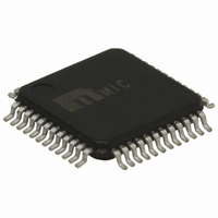
MIC2592B-2BTQ Micrel Inc, MIC2592B-2BTQ Datasheet - Page 17

MIC2592B-2BTQ
Manufacturer Part Number
MIC2592B-2BTQ
Description
IC CTRLR HOTPLUG PCI DUAL 48TQFP
Manufacturer
Micrel Inc
Type
Hot-Swap Controllerr
Datasheet
1.MIC2592B-2YTQ.pdf
(31 pages)
Specifications of MIC2592B-2BTQ
Applications
General Purpose, PCI Express
Internal Switch(s)
No
Voltage - Supply
3.3V, 12V
Operating Temperature
0°C ~ 70°C
Mounting Type
Surface Mount
Package / Case
48-TQFP
Lead Free Status / RoHS Status
Contains lead / RoHS non-compliant
Available stocks
Company
Part Number
Manufacturer
Quantity
Price
Inrush Current and Load Dominated Start-up
The expected maximum inrush current can be calculated by
using the following equation:
where I
or I
C
MOSFET and any external capacitance connected from
the GATE output pin to the GATE reference – GND or
source).
For the 3.3V outputs and 12V outputs (if no external 12VGATE
output capacitors are implemented), the following equation
is used to determine the output slew rate.
Consequently, the overcurrent timer delay must be pro-
grammed to exceed the time it will take to charge the output
load to the input rail voltage level.
MAIN Outputs (Start-up Delay and Slew-Rate Control)
The 3.3V outputs act as source followers. In this mode of
operation,V
output reaches 3.3V. The voltage on the gate of the MOSFET
output reaches 3.3V. The voltage on the gate of the MOSFET
will then continue to rise until it reaches 12V, which ensures
minimum R
command to a slot and the appearance of voltage at the slot’s
command to a slot and the appearance of voltage at the slot’s
3.3V output. This delay is the time required to charge the
3VGATE output up to the threshold voltage of the external
MOSFET (typically about 3V).
The source (output) side of the external MOSFET will reach
the drain voltage in a time given by:
For the 12V outputs, each MOSFET is confi gured as a Miller
integrator (by virtue of C
the MOSFET’s gate and drain). In this confi guration, the
feedback action from drain to gate of the MOSFET causes
the voltage at the drain of the MOSFET to slew in a linear
fashion at a rate which satisfi es the following equation:
A delay exists between the ON command to a slot and the
appearance of voltage at the slot’s 12V output. For a slot’s
12V output, that delay is given by the time required for the
capacitor from the gate of the MOSFET to its source (typically
fi ve times the value of C
voltage of the MOSFET (typically about 3V). In this instance,
the delay before the output voltage starts ramping can be
approximated by:
March 2005
GATE
GATE(12VSINK)
GATE(12VSINK)
GATE(12VSINK)
INRUSH
is the total GATE capacitance (C
is the total GATE capacitance (C
GATE
dV
t
t
3VDLY
3V(SOURCE_DRAIN)
DS(ON)
DS(ON)
DS(ON)
SOURCE
OUT
is the GATE pin current, I
, C
I
dt
GATE
dv / dt(12V)
. Note that a delay exists between the ON
C
I
LOAD
GATE(3VCHARGE)
= [V
GATE
C
I
LOAD 3V 12V
LIM 3V 12V
MILLER
GATE
C
C
MILLER
is the load capacitance, and
is the load capacitance, and
LOAD
GATE
V
GS(TH)
t
– V
3VDLY
, which is connected between
) to charge to the threshold
C
TH(ON)
TH(ON)
TH(ON)
25 A
I
MILLER
GATE
C
] until the associated
LOAD
ISS
C
C
GATE(3VCHARGE)
GATE(3VCHARGE)
GATE(3VCHARGE)
LOAD
GAT E
I
LIM(3V)
of the external
V
DRAIN
17
where C
MOSFET, any external capacitance from the GATE output of
MOSFET, any external capacitance from the GATE output of
the MIC2592B to the source of the MOSFET, and C
(external, if used).
Table 1 approximates the output slew-rate for various values
of C
(external C
ternal MOSFET for the 3.3V rail; C
*
Power-Down Cycle
When one or more PCI slots are disabled via the MIC2592B
output control pins, ON[A/B] or AUXEN[A/B], the output volt-
age for each supply will discharge as a function of the RC
time constant produced by the controller’s internal resistance
(R
(C
in the Electrical Characteristics Table. The charts below in
Figure 7 display curves of the fall time (90% - 10%) as a
function of the output load capacitance for both the 3V and
12V MAIN outputs.
Standby Mode
Standby mode is entered when one or more of the MAIN
supply inputs (12VIN and/or 3VIN) is below its respective
UVLO threshold or OFF. The MIC2592B also supplies
3.3V auxiliary outputs (VAUX[A/B]), satisfying PCI Express
specifi cations. These outputs are fed via the VSTBY[A/B]
input pins and controlled by the AUXEN[A/B] input pins
or via their respective bits in the Control Registers. These
Table 1. 3.3V and 12V Output Slew-Rate Selection for
DIS
LOAD
C
1200
1000
Figure 7. 3V and 12V Output Discharge vs. Load
800
600
400
200
Values in this range will be affected by the internal parasitic capaci-
tances of the MOSFETs used, and should be verifi ed experimentally.
GATE
GATE
Function of Load Capacitance
) connected to the output and the load capacitance
0
0
0
0
0
0
0
3V Output Discharge as a
). The typical value of R
0.022µF*
0.022µF*
0.022µF*
0.047µF
0.047µF
0.047µF
0.01µF*
0.01µF*
0.01µF*
GATE(TOTAL)
GATE(TOTAL)
GATE(TOTAL)
0.1µF
0.1µF
0.1µF
Gate Capacitance Dominated Start-up
when start-up is dominated by GATE capacitance
5
5
50
5
or C
t
0
12
GATE
FALL TIME (ms)
VDLY
100
MILLER
from GATE pin to ground plus C
150
C
| I
is the sum of the C
200
GATE(TOTAL)
GATE
Capacitance
250
I
| = 25µA
GATE
DIS
1200
1000
800
600
400
200
V
Function of Load Capacitance
MILLER
0
0
0
GS(TH)
0
0
12V Output Discharge as a
for each supply is listed
dv/dt (load)
dv/dt (load)
0.532 V/ms
0.532 V/ms
0.532 V/ms
1.136V/ms
1.136V/ms
1.136V/ms
0.250V/ms
0.250V/ms
0.250V/ms
2.5V/ms
2.5V/ms
2.5V/ms
500
GS
FALL TIME (ms)
for the 12V rail).
1000 1500 2000 2500
of the external
GS
M9999-033105
of the ex-
MILLER


