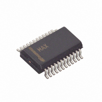
MAX5929AEEG+ Maxim Integrated Products, MAX5929AEEG+ Datasheet

MAX5929AEEG+
Specifications of MAX5929AEEG+
Related parts for MAX5929AEEG+
MAX5929AEEG+ Summary of contents
Page 1
... Internal Charge Pumps Generate n-Channel MOSFET Gate Drives o Inrush Current Regulated at Startup o Autoretry or Latched Fault Management o Programmable Undervoltage Lockout o Status Outputs Indicate Fault/Safe Condition PART MAX5927AETJ+ MAX5929AEEG+ MAX5929BEEG+ MAX5929CEEG+ MAX5929DEEG Exposed pad. + Denotes a lead-free/RoHS-compliant package. Selector Guide and Typical Operating Circuit appear at end of data sheet. ...
Page 2
Low-Voltage, Quad, Hot-Swap Controllers/Power Sequencers ...
Page 3
ELECTRICAL CHARACTERISTICS (continued +1V to +15V provided at least one supply is larger than or equal to +2.7V, T IN_ Typical values are 12.0V, V IN1 IN2 PARAMETER SYMBOL MOSFET DRIVER Startup Period (Note 5) ...
Page 4
Low-Voltage, Quad, Hot-Swap Controllers/Power Sequencers ELECTRICAL CHARACTERISTICS (continued +1V to +15V provided at least one supply is larger than or equal to +2.7V, T IN_ Typical values are 12.0V, V IN1 IN2 PARAMETER SYMBOL LOGIC ...
Page 5
Typical Operating Circuit , Fairchild FDB7090L, V +25°C, unless otherwise noted. Channels 1 through 4 are identical in performance. Where characteristics are interchangeable, channels 1 through 4 are referred to as ...
Page 6
Low-Voltage, Quad, Hot-Swap Controllers/Power Sequencers ( Typical Operating Circuit , Fairchild FDB7090L, V +25°C, unless otherwise noted. Channels 1 through 4 are identical in performance. Where characteristics are interchangeable, channels 1 through ...
Page 7
Typical Operating Circuit , Fairchild FDB7090L, V +25°C, unless otherwise noted. Channels 1 through 4 are identical in performance. Where characteristics are interchangeable, channels 1 through 4 are referred to as ...
Page 8
Low-Voltage, Quad, Hot-Swap Controllers/Power Sequencers PIN NAME MAX5929A– MAX5927A MAX5929D 1 4 IN1 2 5 SENSE1 3 6 GATE1 4 — LIM4 5 7 IN4 6 8 SENSE4 7 9 GATE4 8 10 STAT1 9 11 STAT2 10 12 TIM ...
Page 9
PIN NAME MAX5929A– MAX5927A MAX5929D 22 20 GATE2 23 21 SENSE2 24 22 IN2 25 — LIM2 26 23 ON4 27 24 ON3 28 1 MODE 29 — POL 30 2 ON2 31 3 ON1 32 — LIM1 EP — ...
Page 10
Low-Voltage, Quad, Hot-Swap Controllers/Power Sequencers R LIM1 LIM1* IN1 V V SC SENSE1 FAST COMP. SENSE1 SLOW COMP. GATE1 CHARGE Q1 PUMP OUT1 SLOW DISCHARGE FAST DISCHARGE 3mA/ 50mA 100μA STAT1 LIM3* R LIM3 IN3 V ...
Page 11
ON1 ON2 ON3 ON4 ANY IN_ IN2 IN3 IN4 *THE OUT_ DISCHARGE RATE IS A RESULT OF NATURAL DECAY OF THE LOAD RESISTANCE AND CAPACITANCE. Figure 2. Voltage-Tracking Timing Diagram (Provided ...
Page 12
Low-Voltage, Quad, Hot-Swap Controllers/Power Sequencers ON1 ON2 ON3 ON4 ANY IN_ IN2 IN3 IN4 OUT1 OUT2 OUT3 OUT4 *THE OUT_ DISCHARGE RATE IS A RESULT OF NATURAL DECAY OF THE LOAD RESISTANCE AND CAPACITANCE. Figure 3. Power-Sequencing Timing Diagram (Provided ...
Page 13
ON1 = ON2 = ON3 = ON4 OVERCURRENT FAULT CONDITION OUT1 OUT2 OUT3 OUT4 *THE OUT_ DISCHARGE RATE IS A RESULT OF NATURAL DECAY OF THE LOAD RESISTANCE AND CAPACITANCE. Figure 4. Power-Sequencing Fault Turn-Off The MAX5927A/MAX5929A–MAX5929D turn off all ...
Page 14
Low-Voltage, Quad, Hot-Swap Controllers/Power Sequencers ON1 ON2 ON3 ON4 IN1 IN2 IN3 IN4 t D, UVLO OUT1 OUT2 OUT3 OUT4 * THE OUT_ DISCHARGE RATE IS A RESULT OF NATURAL DECAY OF THE LOAD RESISTANCE AND CAPACITANCE. Figure 5. Independent ...
Page 15
ON_ STAT_ t START GATE_ V OUT_ V FC,TH R SENSE_ I LOAD_ t ON Figure 6. Independent Mode Startup Waveforms Slow-Comparator Startup Period The slow comparator is disabled during the startup period while the external MOSFETs ...
Page 16
Low-Voltage, Quad, Hot-Swap Controllers/Power Sequencers Table 2. Selecting Fault Management Mode (MAX5927A) LATCH FAULT MANAGEMENT Unconnected Fault condition latches MOSFETs off Low Autoretry mode Table 3. Selecting STAT_ Polarity (MAX5927A) POL Low Asserts low Unconnected Asserts high (open drain) t ...
Page 17
Table 4. Status Output Truth Table: Voltage-Tracking and Power-Sequencing Modes CHANNEL 1 PART FAULT Yes X MAX5927A (POL = 1), MAX5929B/ X MAX5929D X No Yes X MAX5927A (POL = X 0), MAX5929C/ X MAX5929D Low, ...
Page 18
Low-Voltage, Quad, Hot-Swap Controllers/Power Sequencers Table 6. Recommended n-Channel MOSFETs PART NUMBER IRF7413 IRF7401 IRL3502S MMSF3300 MMSF5N02H MTB60N05H FDS6670A ND8426A FDB8030L Table 7. Component Manufacturers COMPONENT MANUFACTURER Vishay/Dale Resistors Sense Resistors IRC, Inc. International Rectifier MOSFETs Fairchild Semiconductor On Semiconductor ...
Page 19
R SENSE_ V IN_ R PULLUP IN_ SENSE_ MAX5927A STAT_ MAX5929A MAX5929B MAX5929C ON_ MAX5929D GND Figure 9. Operating with an External Gate Capacitor Startup Sequence There are two ways of completing the startup sequence. Case A describes a startup ...
Page 20
Low-Voltage, Quad, Hot-Swap Controllers/Power Sequencers OFF GND V Z Figure 11. Power Sequencing: Channel Z Turns On t With a 22nF gate capacitor, the inrush current, charge, and discharge times are: μ ...
Page 21
The maximum inrush current in this case is INRUSH R SENSE Figure 6 shows the waveforms and timing diagrams for a startup transient with current regulation (see the Typical Operating Characteristics ). When operating ...
Page 22
Low-Voltage, Quad, Hot-Swap Controllers/Power Sequencers Layout Considerations To take full tracking advantage of the switch response time to an output fault condition important to keep all traces as short as possible and to maximize the high-current trace dimensions ...
Page 23
... PART MAX5927AETJ+ Programmable MAX5929AEEG+ Fixed MAX5929BEEG+ Fixed MAX5929CEEG+ Fixed MAX5929DEEG+ Fixed Pin Configurations (continued) TOP VIEW + MODE 1 ON2 2 ON1 3 IN1 4 MAX5929A– SENSE1 5 MAX5929D GATE1 6 IN4 7 SENSE4 8 GATE4 9 STAT1 10 STAT2 11 TIM 12 QSOP Maxim cannot assume responsibility for use of any circuitry other than circuitry entirely embodied in a Maxim product. No circuit patent licenses are implied ...


