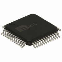
MIC2593-2YTQ TR Micrel Inc, MIC2593-2YTQ TR Datasheet - Page 15

MIC2593-2YTQ TR
Manufacturer Part Number
MIC2593-2YTQ TR
Description
IC PCI HOT PLUG CTLR DUAL 48TQFP
Manufacturer
Micrel Inc
Type
Hot-Swap Controllerr
Datasheet
1.MIC2593-2YTQ.pdf
(26 pages)
Specifications of MIC2593-2YTQ TR
Applications
PCI, PCI-X
Internal Switch(s)
No
Voltage - Supply
3.3V, 5V, ±12V
Operating Temperature
0°C ~ 70°C
Mounting Type
Surface Mount
Package / Case
48-TQFP
Lead Free Status / RoHS Status
Lead free / RoHS Compliant
Other names
MIC2593-2YTQTR
MIC2593-2YTQTR
MIC2593-2YTQTR
Either or both external ON[A/B] and AUXEN[A/B] input
signals are asserted, AND
In order to clear /FAULT[A/B] outputs once asserted,
ON[A/B] and/or AUXEN[A/B] input signals must be de-
asserted. Please see the /FAULT[A/B] pin description for
additional information.
Hot Plug Interface (HPI) Operation
Once the input supplies are above their respective UVLO
thresholds, the Hot Plug Interface can be utilized for
power control by enabling the control input pins
(AUXEN[A/B] and ON[A/B]) for each slot. In order for the
MIC2593 to switch on the VAUX supply for either slot, the
AUXEN[A/B] control must be enabled after the power-on-
reset delay, t
output supplies can also be enabled after t
response diagram of Figure 8 illustrates a Hot Plug
Interface operation where an overcurrent fault is detected
by the MIC2593 controller after initiating a power-up
sequence. The figure illustrates the output response of
/FAULT, /INT, VAUX[A/B] supplies, and an external
MOSFET control MAIN[A/B] output supply, either 3.3V or
5V.
MIC2593 SMBus Address Configuration
The MIC2593 responds to its own unique address which
is assigned using A2, A1, and A0. These represent the 3
LSBs of its 7-bit address, as shown in Table 3. These
address bits are assigned only during power up of the
VSTBY[A/B] supply input. These three bits allow up to
eight MIC2593 devices in a single system. These pins
are either grounded or left unconnected to specify a
logical 0 or 1, respectively. A pin designated as a logical
1 may also be pulled up to V
Micrel, Inc.
September 2008
•
•
•
•
•
12VIN[A/B], 12MVIN[A/B], 5VIN[A/B], 3VIN[A/B],
or VSTBY[A/B] input voltage is lower than its
respective ULVO threshold, OR
The fast OC circuit breaker[A/B] has tripped, OR
The slow OC circuit breaker[A/B] has tripped
AND its filter timeout[A/B] has expired, OR
The slow OC circuit breaker[A/B] has tripped
AND Slot[A/B] die temperature exceeds 140°C,
OR
The
exceeds160°C
POR
MIC2593’s
(typically 500µs), has elapsed. The MAIN
STBY
global
.
die
POR
temperature
. The timing
15
Serial Port Operation
The MIC2593 uses standard SMBus Write_Byte and
Read_Byte operations for communication with its host.
The SMBus Write_Byte operation involves sending the
device’s slave address, with the R/W bit (LSB) set to the
low (write) state, followed by a command byte and a
data byte. The SMBus Read_Byte operation is similar,
but is a composite write and read operation: the host first
sends the device’s slave address followed by the
command byte, as in a write operation. A new “Start” bit
must then be sent to the MIC2593, followed by a repeat
of the slave address with the R/W bit set to the high
(read) state. The data to be read from the part may then
be clocked out. There is one exception to this rule: If the
location latched in the pointer register from the last write
operation is known to be correct (i.e., points to the
desired
“Receive_Byte” procedure may be used. To perform a
Receive_Byte operation, the host sends an address byte
to select the slave MIC2593, with the R/W bit set to the
high (read) state, and then retrieves the data byte.
Figures 9 through 11 show the formats for these data
read and data write procedures.
The Command Register is eight bits (one byte) wide.
This byte carries the address of the MIC2593’s register
to be operated upon. The command byte values
corresponding
addresses are shown in Table 4. Command byte values
other than 0000 0XXXb = 00h - 07hare reserved and
should not be used.
A2
0
0
0
0
1
1
1
1
Inputs
register
Table 3. MIC2593 SMBus Addressing
A1
0
0
1
1
0
0
1
1
to
A0
0
1
0
1
0
1
0
1
within
the
MIC2593 Slave Addresses
1000 000
1000 001
1000 010
1000 011
1000 100
1000 101
1000 110
1000 111
Binary
various
the
b
b
b
b
b
b
b
b
MIC2593),
MIC2593
M9999-092208
Hex
8A
8C
8E
80
82
84
86
88
h
h
h
h
h
h
h
h
MIC2593
then
register
the


