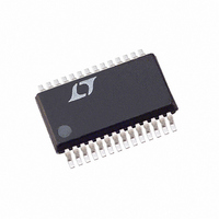
LTC4261IGN Linear Technology, LTC4261IGN Datasheet - Page 22

LTC4261IGN
Manufacturer Part Number
LTC4261IGN
Description
IC CTRLR HOTSWAP W/ADC 28-SSOP
Manufacturer
Linear Technology
Type
Hot-Swap Controllerr
Datasheet
1.LTC4261IGNPBF.pdf
(32 pages)
Specifications of LTC4261IGN
Applications
General Purpose
Internal Switch(s)
No
Voltage - Supply
9 V ~ 11.2 V
Operating Temperature
-40°C ~ 85°C
Mounting Type
Surface Mount
Package / Case
28-SSOP (0.150", 3.95mm Width)
Family Name
LTC4261
Package Type
SSOP N
Operating Supply Voltage (min)
-12V
Operating Supply Voltage (max)
-100V
Operating Temperature (min)
-40C
Operating Temperature (max)
85C
Operating Temperature Classification
Industrial
Product Depth (mm)
3.99mm
Product Height (mm)
1.5mm
Mounting
Surface Mount
Pin Count
28
Lead Free Status / RoHS Status
Contains lead / RoHS non-compliant
Lead Free Status / RoHS Status
Contains lead / RoHS non-compliant
Available stocks
Company
Part Number
Manufacturer
Quantity
Price
Company:
Part Number:
LTC4261IGN
Manufacturer:
LT
Quantity:
1 905
Part Number:
LTC4261IGN
Manufacturer:
LINEAR/凌特
Quantity:
20 000
Company:
Part Number:
LTC4261IGN#PBF
Manufacturer:
LINEAR
Quantity:
1 530
Part Number:
LTC4261IGN#PBF
Manufacturer:
LINEAR/凌特
Quantity:
20 000
Part Number:
LTC4261IGN-2
Manufacturer:
LINEAR/凌特
Quantity:
20 000
Company:
Part Number:
LTC4261IGN-2#PBF
Manufacturer:
LINEAR
Quantity:
542
Part Number:
LTC4261IGN-2#PBF
Manufacturer:
LINEAR/凌特
Quantity:
20 000
LTC4261/LTC4261-2
APPLICATIONS INFORMATION
Confi guring the PGIO Pin
Table 6 describes the possible states of the PGIO pin us-
ing the CONTROL register bits D6 and D7. At power-up
the default state is for the PGIO pin to pull low when
the second power good signal is ready. Other uses for
the PGIO pin are to go high impedence when the sec-
ond power good is ready, a general purpose output and a
general purpose input. When the PGIO pin is confi gured
as a general purpose output, the status of bit C6 is sent
out to the pin. When it is confi gured as a general pur-
pose input, if the input voltage at PGIO is higher than
1.25V, both bit A6 in the STATUS register and bit B6 in
the FAULT register are set. If the input voltage at PGIO
subsequently drops below 1.25V, bit A6 is cleared. Bit
B6 can be cleared by resetting the FAULT register as de-
scribed previously.
Design Example
As a design example, consider the 200W application with
C
range is from 43V to 71V with a UV turn-off threshold of
38.5V.
The design fl ow starts with calculating the maximum in-
put current:
where 36V is the minimum input voltage.
The selection of the sense resistor, R
the minimum current limit threshold and maximum input
current:
The inrush current is set to 0.66A using C
The value of R
discussed previously.
22
L
I
R
C
= 330µF as shown in Figure 1. The operating voltage
MAX
R
S
=
=
=
C
∆
L
200
V
36
•
SENSE MIN
I
I
MAX
I
INRUSH
V
RAMP
W
F
and C
(
=
5 6 .
=
)
F
A
=
330
are chosen to 1k and 33nF as
45
5 6
.
µF
mV
A
•
0 66
=
20
.
8
µA
m
S
A
Ω
, is determined by
=
10
R
:
nF
The FET is selected to handle the maximum power dissi-
pation during start-up or an input step. The latter usually
results in a larger power due to summation of the inrush
current charging C
step, the total P
where t is the time it takes to charge up C
which gives a P
Now the P
curves of candidate FETs must be lower than 244W
The SOA curves of the IRF1310NS provide for 5A at 50V
(250W) for 10ms, which gives a P
satisfi es the requirement.
Sizing R1, R2 and R3 for the required UV and OV thresh-
old voltages:
Layout Considerations
To achieve accurate current sensing, a Kelvin connection
is recommended. The minimum trace width for 1oz cop-
per foil is 0.02" per amp to make sure the trace stays at a
reasonable temperature. Using 0.03" per amp or wider is
recommended. Note that 1oz copper exhibits a sheet re-
sistance of about 530µΩ/square. Small resistances add
up quickly in high current applications. To improve noise
immunity, put the resistive divider to the UV and OV pins
close to the chip and keep traces to V
A 0.1µF capacitor from the UVH or UVL pin (and OV pin
through resistor R2) to V
V
V
V
V
P t
t
UV(RISING)
UVH(TH)
OV(RISING)
OV(TH)
2
=
C
=
I
L
INRUSH
(
36
•
= 1.77V rising and 1.7325V falling)
36
2
= 2.56V and V
t given by the SOA (safe operating area)
V I
V
•
= 72.3V, V
2
= 43V, V
2
MAX
=
t value of 244W
t in the FET is approximated by:
L
330
and the load current. For a 36V input
)
2
0 66
µF
.
•
3
EE
t
•
UVH(TH)
UV(FALLING)
A
36
OV(FALLING)
helps reject supply noise.
V
2
=
s.
2
= 2.291V)
18
t value of 625W
ms
= 38.5V, (using
IN
= 70.7V (using
L
and V
:
EE
2
short.
s and
42612fb
2
s.


