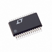
LTC4240CGN#PBF Linear Technology, LTC4240CGN#PBF Datasheet - Page 13

LTC4240CGN#PBF
Manufacturer Part Number
LTC4240CGN#PBF
Description
IC CTLR HOT SWAP CPCI I2C 28SSOP
Manufacturer
Linear Technology
Type
Hot-Swap Controllerr
Datasheet
1.LTC4240CGNPBF.pdf
(28 pages)
Specifications of LTC4240CGN#PBF
Applications
CompactPCI™
Internal Switch(s)
No
Voltage - Supply
3.3V, 5V, ±12V
Operating Temperature
0°C ~ 70°C
Mounting Type
Surface Mount
Package / Case
28-SSOP (0.150", 3.95mm Width)
Lead Free Status / RoHS Status
Lead free / RoHS Compliant
Available stocks
Company
Part Number
Manufacturer
Quantity
Price
APPLICATIO S I FOR ATIO
START and STOP Commands
The START command is defined as a high to low transition
of the SDA line while the SCL line is high. It is an asynchro-
nous event issued by the host, waking up all slave devices
and alerting them that a slave address is being written onto
the bus. Only the slave device that matches the address will
communicate with the host. The STOP command is de-
fined as a low to high transition on the SDA line while SCL
is high. It is also an asynchronous event issued by the host
to signal the termination of the data transfer. Other than
START and STOP commands, the SDA line is allowed to
change states only when SCL is low.
Address Byte
Once the LTC4240 has detected a START command, it
clocks in the SDA line on the succeeding 9 SCL rising
edges. The first 7 bits clocked in contain the address of the
slave device targeted by the host. The first (MSB) address
bit must be set to low and the second bit must be set to
high. The next 5 bits are fed into a digital comparator and
compared against the output of an internal 5-bit A/D. If the
comparison is true, then there is an address match and the
LTC4240 continues to communicate with the host device.
The LTC4240 proceeds to acknowledge the address match
by pulling the SDA line low while SCL is low, just before the
9th SCL rising edge. Figures 1 and 3 show a timing
diagram of the START condition and address byte for both
the Send Byte and Receive Byte protocols. Note that the
SDA bit clocked in with the 8th SCL edge determines
whether the host is sending or receiving information to/
from the LTC4240.
Send Byte Protocol
The Send Byte protocol allows a host to write information
into the LTC4240 and command the LTC4240 to perform
certain predetermined functions. The host initiates com-
munication with a START bit followed by 7 address bits.
The address bits are followed by the R/W bit, which is low
for Send Byte. The 9th bit is asserted low by the LTC4240
U
U
W
U
to acknowledge when there has been an address match.
The only time the LTC4240 writes data onto the SDA bus
during a send byte is to acknowledge the address and
command bytes. The first 8 bits are referred to collectively
as the address byte.
The command byte follows the address byte. The
command byte contains the information sent from the
host to the LTC4240. After the LTC4240 acknowledges the
address byte, each of the next 8 SCL rising edges shifts
SDA from the host into a shift register inside the LTC4240.
The first 2 bits clocked into the shift register (2 MSBs of the
command latch) are not used by the LTC4240. Only the 6
LSBs are stored in the command latch on the falling edge
of the 8th clock during the command byte. The output of
the command latch remains fixed until the next Send Byte
command overwrites it. Note that if power is turned off
(5V
Figure 1 shows the timing diagram of the entire send byte
protocol. Transmission ends when the host issues a STOP
command. Table 2 defines the functions of the 6 command
bits. Note that some of these functions can override, or can
be overridden by, other circuitry and pins of the LTC4240.
Figure 2 shows the relationship between bits C1 to C3 and
other LTC4240 signals.
Receive Byte Protocol
The Receive Byte protocol is used by the host to read data
from the LTC4240 data latch. This protocol begins with a
START command, issued by the host, followed by 7
address bits. The address bits are followed by the R/W bit,
which is high for Receive Byte. The 9th bit is used by the
LTC4240 to acknowledge when there is an address match.
The data byte then follows the address byte. This byte
contains LTC4240 status information. After the LTC4240
acknowledges the address byte, it shifts 8 bits of data onto
the SDA line. Figure 3 shows the entire Receive Byte timing
diagram. Note that neither the host or the slave acknowl-
edges the data byte (SDA line stays high during 9th clock
edge of the data byte).
IN
< 2V), the command and data latches will be cleared.
LTC4240
13
4240f


