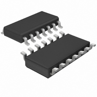
LTC1645CS Linear Technology, LTC1645CS Datasheet - Page 15

LTC1645CS
Manufacturer Part Number
LTC1645CS
Description
IC CTRLR SEQ HOTSWAP DUAL 14SOIC
Manufacturer
Linear Technology
Type
Hot-Swap Controllerr
Datasheet
1.LTC1645CS8PBF.pdf
(24 pages)
Specifications of LTC1645CS
Applications
General Purpose
Internal Switch(s)
No
Voltage - Supply
1.2 V ~ 12 V
Operating Temperature
0°C ~ 70°C
Mounting Type
Surface Mount
Package / Case
14-SOIC (0.154", 3.90mm Width)
Linear Misc Type
Positive Low Voltage
Family Name
LTC1645
Package Type
SOIC N
Operating Supply Voltage (min)
1.2V
Operating Supply Voltage (max)
12V
Operating Temperature (min)
0C
Operating Temperature (max)
70C
Operating Temperature Classification
Commercial
Product Depth (mm)
3.99mm
Product Height (mm)
1.5mm
Mounting
Surface Mount
Pin Count
14
Lead Free Status / RoHS Status
Contains lead / RoHS non-compliant
Lead Free Status / RoHS Status
Contains lead / RoHS non-compliant
Available stocks
Company
Part Number
Manufacturer
Quantity
Price
Part Number:
LTC1645CS
Manufacturer:
LINEAR/凌特
Quantity:
20 000
Part Number:
LTC1645CS#TRPBF
Manufacturer:
LINEAR/凌特
Quantity:
20 000
Part Number:
LTC1645CS8
Manufacturer:
LINEAR/凌特
Quantity:
20 000
Part Number:
LTC1645CS8#TRPBF
Manufacturer:
LT/凌特
Quantity:
20 000
APPLICATIO S I FOR ATIO
This circuit guarantees that: (1) V
V
than V
V
turns off Q1 and Q2 simultaneously. Charge remains
stored on C
vary depending on the loads. D1 and D2 turn on at 1V
( 0.5V each), ensuring condition 1 is satisfied, while D3
prevents violations of condition 2. Different diodes may be
necessary for different output voltage configurations.
Barring an overvoltage condition at the input(s), the only
time these diodes might conduct current is during a
power-down event, and then only to discharge C
C
causes excess current to flow, the circuit breaker will trip
if the current limit level is set appropriately.
Figure 17 shows an application circuit where V
ramps up before V
D1 is reverse-biased, thus the voltage at the ON pin is
determined only by V
and R2. The voltage at the ON pin exceeds 0.8V if V
above 4.6V and V
cycle. As V
and pulls the ON pin above 2V when V
turns on GATE2 and V
monitors V
V
OUT2
OUT2
LOAD2
OUT1
OUT1
by more than 1.2V, and (2) V
with R
ramp up together. On power-down, the LTC1645
. In the case of an input overvoltage condition that
OUT1
LOAD1
by more than 0.4V. On power-up, V
OUT2
HYST
, and the spare comparator monitors
ramps up, D1 becomes forward-biased
and C
OUT1
creating 50mV of hysteresis.
OUT2
U
CC1
OUT2
LOAD2
. V
begins to ramp up after a timing
5V/DIV
5V/DIV
5V/DIV
5V/DIV
2V/DIV
5V/DIV
TIMER
RESET
V
V
through the resistor divider R1
U
OUT1
OUT2
OUT1
V
V
ramps up. The FB comparator
IN2
IN1
and the output voltages will
is initially discharged and
Figure 16. Ramping 3.3V and 2.5V Up and Down Together
W
OUT2
OUT1
OUT1
is never greater
never exceeds
U
4.5V. This
OUT1
LOAD1
CC1
OUT1
and
or
is
Power Supply Multiplexer
Using back-to-back FETs, the LTC1645 can Hot Swap two
supplies to the same output, automatically selecting the
primary supply if present or the secondary supply if the
primary supply is not available. Referring to Figure 18, a
diode-or circuit provides power to the LTC1645 if either
supply is up. Schottky diodes are used to prevent the
voltage at V
out threshold. This application assumes that if a supply is
not present, the supply input is floating.
If only the 3.3V supply is present, the voltage at the COMP
pin is below the trip point and COMPOUT pulls the base of
Q3 low, allowing the GATE1 pin to ramp up normally. The
voltage at the ON pin exceeds 0.8V if the 3.3V supply is
greater than 3V, ramping up GATE1 and turning on Q1A and
Q1B. The ON pin does not exceed 2V (unless the 3.3V supply
exceeds 7.5V!), keeping GATE2 low and Q2A and Q2B off.
If only the 5V supply is present or if both supplies are
present, the COMP
allows the base of Q3 to be pulled high by R2. This turns
Q3 on, keeping GATE1 low and Q1A and Q1B off. The
voltage at the ON pin is pulled above 2V by R1 and GATE2
turns Q2A and Q2B on.
CC1
from approaching the undervoltage lock-
+
pin is above 1.238V and COMPOUT
LTC1645
15
1645fa
+


