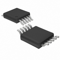
LTC4252A-1IMS#PBF Linear Technology, LTC4252A-1IMS#PBF Datasheet - Page 10

LTC4252A-1IMS#PBF
Manufacturer Part Number
LTC4252A-1IMS#PBF
Description
IC CNTRLR HOTSWAP NEGVOLT 10MSOP
Manufacturer
Linear Technology
Type
Hot-Swap Controllerr
Datasheet
1.LTC4252-1CMS8PBF.pdf
(36 pages)
Specifications of LTC4252A-1IMS#PBF
Applications
General Purpose
Internal Switch(s)
No
Operating Temperature
-40°C ~ 85°C
Mounting Type
Surface Mount
Package / Case
10-TFSOP, 10-MSOP (0.118", 3.00mm Width)
Lead Free Status / RoHS Status
Lead free / RoHS Compliant
Available stocks
Company
Part Number
Manufacturer
Quantity
Price
LTC4252-1/LTC4252-2
LTC4252A-1/LTC4252A-2
PIN FUNCTIONS
V
this pin to the negative side of the power supply.
GATE (Pin 6/Pin 5): N-Channel MOSFET Gate Drive Output.
This pin is pulled high by a 58μA current source. GATE is
pulled low by invalid conditions at V
a circuit breaker fault timeout. GATE is actively servoed to
control the fault current as measured at SENSE. A compen-
sation capacitor at GATE stabilizes this loop. A comparator
monitors GATE to ensure that it is low before allowing an
initial timing cycle, GATE ramp-up after an overvoltage
event or restart after a current limit fault. During GATE
start-up, a second comparator detects if GATE is within
2.8V of V
DRAIN (Pin 7/Pin 6): Drain Sense Input. Connecting an
external resistor, R
drain (V
LTC4252A) and current feedback to TIMER. A comparator
detects if DRAIN is below 2.385V and together with the
GATE high comparator sets the PWRGD flag. If V
above V
The current through R
added to TIMER’s 230μA pullup current during a circuit
breaker fault cycle. This reduces the fault time and MOSFET
heating.
OV (Pin 8/Pin7): Overvoltage Input. The active high thresh-
old at the OV pin is set at 6.15V with 0.6V hysteresis. If OV
> 6.15V, GATE pulls low. When OV returns below 5.55V,
GATE start-up begins without an initial timing cycle. The
LTC4252A OV pin is set at 5.09V with 102mV hysteresis.
If OV > 5.09V, GATE pulls low. When OV returns below
4.988V, GATE start-up begins without an initial timing
cycle. If an overvoltage condition occurs in the middle of
an initial timing cycle, the initial timing cycle is restarted
after the overvoltage condition goes away. An overvoltage
condition does not reset the PWRGD flag. The internal UVLO
at V
prevents transients and switching noise from affecting
the OV thresholds and prevents glitches at the GATE pin.
10
EE
(Pin 5/Pin 4): Negative Supply Voltage Input. Connect
IN
always overrides OV. A 1nF to 10nF capacitor at OV
OUT
DRNCL
IN
) allows voltage sensing below 6.15V (5V for
before PWRGD is set (MS package only).
, DRAIN clamps at approximately V
D
, between this pin and the MOSFET’s
D
is internally multiplied by 8 and
(MS/MS8)
IN
(UVLO), UV, OV, or
DRNCL
OUT
is
.
UV (Pin 9/Pin 7): Undervoltage Input. The active low thresh-
old at the UV pin is set at 2.925V with 0.3V hysteresis. If
UV < 2.925V, PWRGD pulls high, both GATE and TIMER
pull low. If UV rises above 3.225V, this initiates an initial
timing cycle followed by GATE start-up. The LTC4252A
UV pin is set at 3.08V with 324mV hysteresis. If UV <
2.756V, PWRGD pulls high, both GATE and TIMER pull
low. If UV rises above 3.08V, this initiates an initial timing
cycle followed by GATE start-up. The internal UVLO at V
always overrides UV. A low at UV resets an internal fault
latch. A 1nF to 10nF capacitor at UV prevents transients
and switching noise from affecting the UV thresholds and
prevents glitches at the GATE pin.
TIMER (Pin 10/Pin 8): Timer Input. TIMER is used to
generate an initial timing delay at start-up and to delay
shutdown in the event of an output overload (circuit
breaker fault). TIMER starts an initial timing cycle when
the following conditions are met: UV is high, OV is low, V
clears UVLO, TIMER pin is low, GATE is lower than V
SS < 0.2V, and V
5.8μA then charges C
charges to V
quickly pulls low and GATE is activated.
If SENSE exceeds 50mV while GATE is high, a circuit
breaker cycle begins with a 230μA pull-up current charging
C
ing this cycle, the timer pull-up has an additional current
of 8 • I
reaches 4V, a 5.8μA pull-down current slowly discharges
the C
V
pulls low and PWRGD pulls high. The LTC4252-1 TIMER
pin latches high with a 5.8μA pull-up source. This latched
fault is cleared by either pulling TIMER low with an external
device or by pulling UV below V
a shutdown cooling cycle following an overcurrent fault.
This cycle consists of 4 discharging ramps and 3 charging
ramps. The charging and discharging currents are 5.8μA
and TIMER ramps between its 1V and 4V thresholds. At
the completion of a shutdown cooling cycle, the LTC4252-2
attempts a start-up cycle.
T
TMRH
. If DRAIN is approximately 7V (6V for LTC4252A) dur-
T
. In the event that C
DRN
threshold, the circuit breaker trips, GATE quickly
. If SENSE drops below 50mV before TIMER
TMRH
SENSE
(4V), the timing cycle terminates, TIMER
T
– V
, generating a time delay. If C
T
EE
eventually integrates up to the
< V
UVLO
CB
. The LTC4252-2 starts
. A pull-up current of
GATEL
425212fc
IN
IN
T
,


