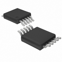
LTC4252A-1CMS Linear Technology, LTC4252A-1CMS Datasheet - Page 15

LTC4252A-1CMS
Manufacturer Part Number
LTC4252A-1CMS
Description
IC CTRLR HOTSWAP NEG VOLT 10MSOP
Manufacturer
Linear Technology
Type
Hot-Swap Controllerr
Specifications of LTC4252A-1CMS
Applications
General Purpose
Internal Switch(s)
No
Operating Temperature
0°C ~ 70°C
Mounting Type
Surface Mount
Package / Case
10-TFSOP, 10-MSOP (0.118", 3.00mm Width)
Family Name
LTC4252A-1
Package Type
MSOP
Operating Temperature (min)
0C
Operating Temperature (max)
70C
Operating Temperature Classification
Commercial
Product Depth (mm)
3mm
Product Height (mm)
0.86mm
Product Length (mm)
3mm
Mounting
Surface Mount
Pin Count
10
Lead Free Status / RoHS Status
Contains lead / RoHS non-compliant
Lead Free Status / RoHS Status
Contains lead / RoHS non-compliant
Available stocks
Company
Part Number
Manufacturer
Quantity
Price
Company:
Part Number:
LTC4252A-1CMS
Manufacturer:
LT
Quantity:
10 000
Company:
Part Number:
LTC4252A-1CMS#TRPBF
Manufacturer:
LINEAR
Quantity:
7 752
APPLICATIONS INFORMATION
and R2 = 32.4k gives a typical operating range of 43.2V
to 82.5V. The undervoltage shutdown and overvoltage
recovery thresholds are then 39.2V and 74.4V. 1% divider
resistors are recommended to preserve threshold accuracy.
The R1-R2 divider values shown in the Typical Application
set a standing current of slightly more than 100μA and
define an impedance at UV/OV of 30kΩ. In most applica-
tions, 30kΩ impedance coupled with 300mV UV hysteresis
makes the LTC4252 insensitive to noise. If more noise
immunity is desired, add a 1nF to 10nF filter capacitor
from UV/OV to V
Separate UV and OV pins are available in the 10-pin MS
package and can be used for a different operating range
such as 35.5V to 76V as shown in Figure 3. Other combi-
nations are possible with different resistor arrangements.
UV/OV COMPARATORS (LTC4252A)
A UV hysteretic comparator detects undervoltage condi-
tions at the UV pin, with the following thresholds:
An OV hysteretic comparator detects overvoltage condi-
tions at the OV pin, with the following thresholds:
UV low-to-high (V
UV high-to-low (V
EE
.
(SHORT PIN)
UV
UV
–48RTN
–48RTN
) = 3.08V
– V
–48V
UVHST
* M0C207
Q2: MMBT5551LT1
464k
10k
34k
Figure 4. – 48V/2.5A Application with Wider Input Operating Range
1%
1%
1%
R1
R2
R3
) = 2.756V
C2
10nF
**DIODES, INC
†
C
0.68μF
RECOMMENDED FOR HARSH ENVIRONMENTS
T
10
9
8
3
OV
TIMER
UV
SS
C
68nF
SS
LTC4252A-1
V
V
EE
IN
5
1
R
10k
1/2W
IN
The UV and OV trip point ratio is designed to match the
standard telecom operating range of 43V to 71V when
connected together as in Figure 2. A divider (R1, R2) is
used to scale the supply voltage. Using R1 = 390k and R2
= 30.1k gives a typical operating range of 43V to 71V. The
undervoltage shutdown and overvoltage recovery thresh-
olds are then 38.5V and 69.6V respectively. 1% divider
resistors are recommended to preserve threshold accuracy.
The R1-R2 divider values shown in Figure 2 set a standing
current of slightly more than 100μA and define an impedance
at UV/OV of 28kΩ. In most applications, 28kΩ impedance
coupled with 324mV UV hysteresis makes the LTC4252A
insensitive to noise. If more noise immunity is desired, add
a 1nF to 10nF filter capacitor from UV/OV to V
The UV and OV pins can be used for a wider operat-
ing range such as 35.5V to 76V as shown in Figure 4.
Other combinations are possible with different resistor
arrangements.
UV/OV OPERATION
A low input to the UV comparator will reset the chip and pull
the GATE and TIMER pins low. A low-to-high UV transition
will initiate an initial timing sequence if the other interlock
PWRGD
SENSE
DRAIN
GATE
OV low-to-high (V
OV high-to-low (V
D
DDZ13B
IN
†
LTC4252A-1/LTC4252A-2
2
7
6
4
**
LTC4252-1/LTC4252-2
22k
C
1μF
R4
IN
R
D
1M
Q2
OV
OV
R5
2.2k
R
10Ω
) = 5.09V
C
– V
C
10nF
100μF
C
*
425212 F04
C
OVHST
L
+
Q1
IRF530S
R
0.02Ω
S
EN
) = 4.988V
LOAD
EE
.
15
425212fc


