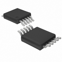
LTC4302CMS-1 Linear Technology, LTC4302CMS-1 Datasheet

LTC4302CMS-1
Specifications of LTC4302CMS-1
Available stocks
Related parts for LTC4302CMS-1
LTC4302CMS-1 Summary of contents
Page 1
... Translates Between 5V and 3.3V Systems (LTC4302-2) Small 10-Pin MSOP Package U APPLICATIO S Live Board Insertion 5V/3.3V Level Translator Servers Capacitance Buffer/Bus Extender Nested Addressing , LTC and LT are registered trademarks of Linear Technology Corporation trademark of Philips Electronics N.V. *U.S. Patent No. 6,650,174 U TYPICAL APPLICATIO 2.7V to 5.5V ...
Page 2
... Operating Temperature Range LTC4302C-1/LTC4302C-2 ...................... LTC4302I-1/LTC4302I-2 .................... – Storage Temperature Range ................. – 125 C + 0.3V Lead Temperature (Soldering, 10 sec).................. 300 ORDER PART NUMBER SDAIN LTC4302CMS-1 SCLIN CONN LTC4302IMS-1 ADDRESS GND MS PART MARKING 10-LEAD PLASTIC MSOP LTYF T JMAX LTYG = 2.7V to 5.5V (LTC4302-2) unless otherwise noted. ...
Page 3
ELECTRICAL CHARACTERISTICS The denotes the specifications which apply over the full operating temperature range, otherwise specifications are 2.7V to 5.5V (LTC4302-1 SYMBOL PARAMETER General Purpose I/Os V I/O Logic Low Voltage ...
Page 4
LTC4302-1/LTC4302 TYPICAL PERFOR A CE CHARACTERISTICS (Specifications are unless otherwise noted Temperature CC 6.1 5 5.7 5.5 5.3 5.1 4.9 V 4.7 CC 4.5 4.3 –40 TEMPERATURE ( ...
Page 5
CTIO S SDAIN (Pin 1): Serial Data Input. Connect this pin to the SDA bus on the backplane. Do not float. SCLIN (Pin 2): Serial Clock Input. Connect this pin to the SCL bus on ...
Page 6
LTC4302-1/LTC4302-2 W BLOCK DIAGRA S SLEW RATE INACC DETECTOR SDAIN 1 SLEW RATE INACC DETECTOR SCLIN 2 + 0.55V CC – 0.45V CC + SDAIN – ADDRESS 4 ADDRESS DECODER 2.5V/ – 2.35V CONN 3 6 ...
Page 7
W BLOCK DIAGRA S SLEW RATE INACC DETECTOR SDAIN 1 SLEW RATE INACC DETECTOR SCLIN 2 + 0.55V CC – 0.45V CC + SDAIN – ADDRESS FILTER 2.5V/ – 2.35V V CC2 + ...
Page 8
LTC4302-1/LTC4302-2 U OPERATIO Live Insertion and Start-Up The LTC4302 allows I/O card insertion into a live back- plane without corruption of the data and clock busses (SDA and SCL). In its main application, the LTC4302 resides on the edge of ...
Page 9
U OPERATIO broken up into 9-bit segments, one byte followed by one bit for acknowledging. For example, sending out an ad- dress consists of 7-bits of device address, 1-bit that signals whether a read or write operation will be per- ...
Page 10
LTC4302-1/LTC4302-2 U OPERATIO Table 1. Suggested ADDRESS 1% Resistor Values (Refer to Figure 1 for R1 and R2) ADDRESS R R 1(TOP) 2(BOTTOM) CODE RESISTOR RESISTOR 00 8660 137 01 2800 137 02 1180 100 03 1370 169 04 1070 ...
Page 11
U OPERATIO th master. The 8 bit of the Address Byte is the Read/Write bit (R/W) and determines whether the master is writing to or reading from the slave. Figure 2 shows a timing diagram of the Start Bit and ...
Page 12
LTC4302-1/LTC4302-2 U OPERATIO Table 3. Register 2 Definition BIT NAME TYPE FUNCTION 7 (MSB) DIR2 Read/Write GPIO2 Mode Output Input* 6 DIR1 Read/Write GPIO1 Mode Output Input 5 OUT CFG2 Read/Write GPIO2 ...
Page 13
U OPERATIO Data Transfer Timing for Write Commands In order to help ensure that bad data is not written into the LTC4302, data from a write command is only stored after a valid Stop Bit has been performed ...
Page 14
LTC4302-1/LTC4302-2 U OPERATIO Connection Circuitry Masters on the SDAIN and SCLIN busses can address the LTC4302 and command it to connect SDAIN to SDAOUT and SCLIN to SCLOUT as described in the “Write One or Two Bytes” section. Once this ...
Page 15
U OPERATIO pulls down the voltage on the 50pF side with a delay of 55ns. This delay is always positive and is a function of supply voltage, temperature and the pull-up resistors and equivalent bus capacitances on both sides of ...
Page 16
LTC4302-1/LTC4302-2 U OPERATIO Glitch Filters The LTC4302 provides glitch filters on both the SDAIN and 2 SCLIN signals as required by the I specification. The filters prevent signals 50ns (minimum) time duration and rail-to-rail voltage magni- tude ...
Page 17
U U APPLICATIO S I FOR ATIO BACKPLANE BACKPLANE CONNECTOR 10k 10k SDA SCL CONN Figure 12. LTC4302 Live Insertion and Capacitance Buffering Application BACKPLANE 10k 10k SDA ...
Page 18
LTC4302-1/LTC4302 APPLICATIO S I FOR ATIO 5V to 3.3V Level Translator and Power Supply Redundancy (LTC4302-2) Systems requiring different supply voltages for the back- plane side and the card side can use the LTC4302-2 as shown in Figure ...
Page 19
... LEAD COPLANARITY (BOTTOM OF LEADS AFTER FORMING) SHALL BE 0.102mm (.004") MAX Information furnished by Linear Technology Corporation is believed to be accurate and reliable. However, no responsibility is assumed for its use. Linear Technology Corporation makes no represen- tation that the interconnection of its circuits as described herein will not infringe on existing patent rights. ...
Page 20
... SMBus Controlled CCFL Switching Regulator 2 LTC1695 SMBus/I C Fan Speed Controller in ThinSOT 2 LTC1840 Dual I C Fan Speed Controller LTC4300A-1/ Hot Swappable 2-Wire Bus Buffers LTC4300A-2 ThinSOT is a trademark of Linear Technology Corporation. Linear Technology Corporation 20 1630 McCarthy Blvd., Milpitas, CA 95035-7417 (408) 432-1900 FAX: (408) 434-0507 C1 0. ...


