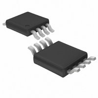
LTC4301IMS8#TR Linear Technology, LTC4301IMS8#TR Datasheet - Page 3

LTC4301IMS8#TR
Manufacturer Part Number
LTC4301IMS8#TR
Description
IC BUFFER BUS HOTSWAP 2WR 8MSOP
Manufacturer
Linear Technology
Type
Hot-Swap Switchr
Datasheet
1.LTC4301CMS8PBF.pdf
(12 pages)
Specifications of LTC4301IMS8#TR
Applications
General Purpose, Buffer/Bus Extender
Internal Switch(s)
Yes
Voltage - Supply
2.7 V ~ 5.5 V
Operating Temperature
-40°C ~ 85°C
Mounting Type
Surface Mount
Package / Case
8-TSSOP, 8-MSOP (0.118", 3.00mm Width)
Lead Free Status / RoHS Status
Contains lead / RoHS non-compliant
Available stocks
Company
Part Number
Manufacturer
Quantity
Price
ELECTRICAL CHARACTERISTICS
temperature range, otherwise specifications are at T
SYMBOL
Input-Output Connection
V
C
I
V
Timing Characteristics
f
t
t
t
t
t
t
Note 1: Stresses beyond those listed under Absolute Maximum Ratings
may cause permanent damage to the device. Exposure to any Absolute
Maximum Rating condition for extended periods may affect device
reliability and lifetime.
TYPICAL PERFOR A CE CHARACTERISTICS
LEAK
I2C,MAX
BUF
HD,STA
SU,STA
SU,STO
HD,DATI
SU,DAT
OS
IN
OL
4.9
4.8
4.7
4.6
4.5
4.4
4.3
4.2
4.1
4.0
3.9
–80
I
CC
–60
vs Temperature
–40
PARAMETER
Input-Output Offset Voltage
Digital Input Capacitance SDAIN, SDAOUT,
SCLIN, SCLOUT
Input Leakage Current
Output Low Voltage, Input = 0V
I
Bus Free Time Between Stop and Start
Condition
Hold Time After (Repeated) Start Condition
Repeated Start Condition Set-Up Time
Stop Condition Set-Up Time
Data Hold Time Input
Data Set-Up Time
2
TEMPERATURE (°C)
–20
C Maximum Operating Frequency
V
V
V
CC
CC
CC
0
= 5.5V
= 3.3V
= 2.7V
20
40
W
60
80
4301 G01
U
100
100
80
60
40
20
0
–50
A
Input – Output High to Low
Propagation Delay vs Temperature
= 25°C. V
C
R
IN
PULLUPIN
CONDITIONS
10k to V
SDA or SCL = 0.2V (Note 2)
(Note 3)
SDA, SCL Pins
SDA, SCL Pins, I
(Note 3)
(Note 3)
(Note 3)
(Note 3)
(Note 3)
(Note 3)
(Note 3)
–25
= C
The
OUT
TEMPERATURE (°C)
= R
= 100pF
●
CC
CC
0
indicates specifications which apply over the full operating
PULLUPOUT
on SDA, SCL, V
V
V
V
= 2.7V to 5.5V, unless otherwise noted.
CC
CC
CC
25
= 2.7V
= 3.3V
= 5.5V
Note 2: The connection circuitry always regulates its output to a higher
voltage than its input. The magnitude of this offset voltage as a function of
the pull-up resistor and V
Characteristics section.
Note 3: Determined by design, not tested in production.
SINK
= 10k
50
= 3mA, V
CC
75
= 3.3V,
CC
4301 G02
= 2.7V
100
CC
●
●
voltage is shown in the Typical Performance
300
250
200
150
100
50
0
0
Connection Circuitry V
MIN
400
0
0
V
10,000
CC
V
CC
= 3.3V
= 5V
TYP
100
600
R
PULLUP
20,000
LTC4301
(Ω)
MAX
OUT
175
100
100
0.4
1.3
10
±5
30,000
0
0
0
– V
T
V
A
IN
= 25°C
= 0V
IN
4301 G03
UNITS
40,000
4301fb
3
kHz
mV
µA
pF
µs
ns
ns
ns
ns
ns
V


