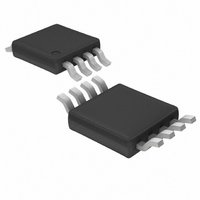
LTC4301CMS8 Linear Technology, LTC4301CMS8 Datasheet - Page 4

LTC4301CMS8
Manufacturer Part Number
LTC4301CMS8
Description
IC BUFFER BUS HOTSWAP 2WR 8MSOP
Manufacturer
Linear Technology
Type
Hot-Swap Switchr
Datasheet
1.LTC4301CMS8PBF.pdf
(12 pages)
Specifications of LTC4301CMS8
Applications
General Purpose, Buffer/Bus Extender
Internal Switch(s)
Yes
Voltage - Supply
2.7 V ~ 5.5 V
Operating Temperature
0°C ~ 70°C
Mounting Type
Surface Mount
Package / Case
8-TSSOP, 8-MSOP (0.118", 3.00mm Width)
Lead Free Status / RoHS Status
Contains lead / RoHS non-compliant
Available stocks
Company
Part Number
Manufacturer
Quantity
Price
Company:
Part Number:
LTC4301CMS8
Manufacturer:
LT
Quantity:
10 000
Part Number:
LTC4301CMS8#PBF
Manufacturer:
LINEAR/凌特
Quantity:
20 000
Company:
Part Number:
LTC4301CMS8#TRPBF
Manufacturer:
MAXIM
Quantity:
6 220
Part Number:
LTC4301CMS8#TRPBF
Manufacturer:
LINEAR/凌特
Quantity:
20 000
PI FU CTIO S
BLOCK DIAGRA
LTC4301
CS (Pin 1): The connection sense pin is a 1.4V threshold
digital input pin. For normal operation CS is grounded.
Driving CS above the 1.4V threshold isolates SDAIN from
SDAOUT and SCLIN from SCLOUT and asserts READY
low.
SCLOUT (Pin 2): Serial Clock Output. Connect this pin to
the SCL bus on the card.
SCLIN (Pin 3): Serial Clock Input. Connect this pin to SCL
on the bus backplane.
GND (Pin 4): Ground. Connect this pin to a ground plane
for best results.
READY (Pin 5): The READY pin is an open drain N-channel
MOSFET output which pulls down when CS is high or
4
U
6
3
1
U
SDAIN
SCLIN
CS
1.8V
1.4V
U
W
R1
200k
LTC4301 Supply Independent 2-Wire Bus Buffer
R2
200k
UVLO
PRECHARGE
CONNECT
PRECHARGE
DELAY
LOGIC
95µs
CONNECT PRECHARGE
CONNECT
when the start-up sequence described in the Operation
section has not been completed. READY goes high when
CS is low and a start-up is complete.
SDAIN (Pin 6): Serial Data Input. Connect this pin to the
SDA bus on the backplane.
SDAOUT (Pin 7): Serial Data Output. Connect this pin to
the SDA bus on the card.
V
of at least 0.01µF close to V
Exposed Pad (Pin 9): Exposed pad may be left open or
connected to device ground.
CC
(Pin 8): Main Input Supply. Place a bypass capacitor
CONNECT
PRECHARGE
CONNECT
CONNECT
CONNECT
R3
200k
CC
R4
200k
for best results.
1.8V
SDAOUT
SCLOUT
READY
GND
V
CC
4301 BD
8
7
2
5
4
4301fb


