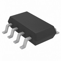
LTC4361ITS8-1#TRPBF Linear Technology, LTC4361ITS8-1#TRPBF Datasheet - Page 7

LTC4361ITS8-1#TRPBF
Manufacturer Part Number
LTC4361ITS8-1#TRPBF
Description
IC CTLR OVP LATCHOFF TSOT23-8
Manufacturer
Linear Technology
Type
Overvoltage and Overcurrent Controllerr
Datasheet
1.LTC4361CDC-2TRMPBF.pdf
(16 pages)
Specifications of LTC4361ITS8-1#TRPBF
Applications
General Purpose
Internal Switch(s)
No
Voltage - Supply
2.5 V ~ 5.5 V
Operating Temperature
-40°C ~ 85°C
Mounting Type
Surface Mount
Package / Case
SOT-23-8 Thin, TSOT-23-8
Lead Free Status / RoHS Status
Lead free / RoHS Compliant
Available stocks
Company
Part Number
Manufacturer
Quantity
Price
APPLICATIONS INFORMATION
The typical LTC4361 application protects 2.5V to 5.5V
systems in portable devices from power supply overvolt-
age. The basic application circuit is shown in Figure 1.
Device operation and external component selection is
discussed in detail in the following sections.
Start-Up
When V
2.1V, the GATE driver is held low and the PWRGD pull-down
is high impedance. When V
held low, a 130ms delay cycle starts. Any undervoltage or
overvoltage event at IN (V
the delay cycle. This delay allows the N-channel MOSFET
to isolate the output from any input transients that occur
at start-up. When the delay cycle completes, GATE starts
its slow ramp-up.
GATE Control
An internal charge pump provides a gate overdrive greater
than 3.5V when 2.5V ≤ V
is guaranteed to be greater than 4.5V. This allows the use
of logic-level N-channel MOSFETs. An internal 6V clamp
between GATE and OUT protects the MOSFET gate.
Figure 1. Protection from Input Overvoltage and Overcurrent
V
5V
IN
IN
is less than the undervoltage lockout level of
R
0.025Ω
SENSE
SENSE
IN
ON
IN
Si1470DH
LTC4361
IN
GATE
GND
< 3V. If V
M1
IN
PWRGD
< 2.1V or V
rises above 2.1V and ON is
OUT
436112 F01
IN
≥ 3V, the gate drive
IN
> 5.7V) restarts
C
10μF
OUT
V
5V
1.5A
OUT
The GATE ramp rate is limited to 3V/ms. V
a similar rate which results in an inrush current into the
load capacitor C
The servo loop is compensated by the parasitic capaci-
tance of the external MOSFET. No further compensation
components are normally required. In the case where
the parasitic capacitance is less than 100pF , a 100pF
compensation capacitor between GATE and ground may
be required.
An even slower GATE ramp and lower inrush current
can be achieved by connecting an external capacitor, C
from GATE to ground. The voltage at GATE then ramps
up with a slope equal to 10μA/C
the formula:
Overvoltage
When power is fi rst applied, V
(V
ramped up to turn on the MOSFET. If V
5.8V (V
30mA fast pull-down on GATE within 1μs. After an over-
voltage condition, the MOSFET is held off until V
again remains below 5.7V for 130ms.
Overcurrent
The overcurrent comparator protects the MOSFET from
excessive current. It trips when the SENSE pin falls more
than 50mV below IN for 10μs. When the overcurrent
comparator trips, GATE is pulled low quickly and the
PWRGD pull-down releases. The LTC4361-2 automatically
tries to apply power again after a 130ms start-up delay.
IN(OV)
I
C
INRUSH
G
=
IN(OV)
I
– ∆V
INRUSH
10µA
= C
LTC4361-1/LTC4361-2
), the overvoltage comparator activates the
OV
OUT
OUT
) for more than 130ms before GATE is
• C
•
OUT
dV
of:
GATE
dt
= C
IN
OUT
G
must remain below 5.7V
[V/s]. Choose C
• 3 mA/µF
IN
[
then rises above
OUT
follows at
]
G
IN
using
436112fa
once
7
G
,


