MCZ34670EG Freescale Semiconductor, MCZ34670EG Datasheet - Page 15

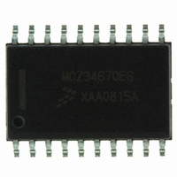
MCZ34670EG
Manufacturer Part Number
MCZ34670EG
Description
IC POE CURR MODE SW REG 20-SOIC
Manufacturer
Freescale Semiconductor
Type
Power Over Ethernet Controller (PoE)r
Datasheet
1.MCZ34670EGR2.pdf
(24 pages)
Specifications of MCZ34670EG
Applications
Remote Peripherals (Industrial Controls, Cameras, Data Access)
Internal Switch(s)
No
Voltage - Supply
60V
Operating Temperature
-40°C ~ 85°C
Mounting Type
Surface Mount
Package / Case
20-SOIC (0.300", 7.50mm Width)
Product
PoE / LAN Solutions
Supply Voltage (max)
80 V
Supply Voltage (min)
- 0.3 V
Power Dissipation
800 mW
Operating Temperature Range
- 40 C to + 85 C
Mounting Style
SMD/SMT
Supply Current
18 mA
Output Current
2.1A
Digital Ic Case Style
SOIC
No. Of Pins
20
Duty Cycle (%)
48%
Uvlo
2V
Frequency
400kHz
Msl
MSL 3 - 168 Hours
Rohs Compliant
Yes
Lead Free Status / RoHS Status
Lead free / RoHS Compliant
Available stocks
Company
Part Number
Manufacturer
Quantity
Price
Part Number:
MCZ34670EG
Manufacturer:
FREESCALE
Quantity:
20 000
Company:
Part Number:
MCZ34670EGR2
Manufacturer:
KODENSHI
Quantity:
6 400
converters running in continuos conduction mode (CCM).
The value of the slope compensation depends on the
switching frequency. See
Table 10. Slope Compensation Values
ISOLATED OPTOCOUPLER FEEDBACK
an optocoupler and a shunt regulator (see
output voltage accuracy is a function of the accuracy of the
shunt regulator and feedback resistor divider tolerance,
therefore the feedback resistors should have an appropriate
accuracy.
secondary side by the optocoupler and a 3-pin adjustable
shunt regulator, the internal error amplifier of the 34670 is not
used. The FB pin is connected to V
internal open-drain error amplifier.
through the internal 5.0 kΩ pull-up resistor between COMP
and an internal 5.0 V reference.
output voltage regulation, the output voltage is set by the ratio
of resistors R
voltage is given by the following equation:
where V
TL431).
Analog Integrated Circuit Device Data
Freescale Semiconductor
Switching Frequency [kHz]
Isolated voltage feedback can be accomplished by using
Since the error amplifier function is implemented on the
The bias voltage for the optocoupler is accomplished
When a TL431 or TLV431 shunt regulator is used for
REF
= 1.24 V for the TLV431 (V
1
100
250
400
and R
V
2
O
, see
=
Table
V
REF
Figure 16
⋅
Slope Compensation [mV/µs]
10.
⎛
⎜
⎝
1
OUT
+
R 1
-------
R 2
for details. The output
, thus disabling the
⎞
⎟
⎠
REF
Figure
10
25
50
= 2.5 V for the
19). The
ISOLATED PRIMARY CONTROL FEEDBACK
of a tertiary winding (see
solution without optocoupler and shunt regulator is clearly the
cost effectiveness. Nevertheless the line and load regulation
is worse than with optocoupler feedback.
compensation components are connected between pins
COMP and FB.
INTERNAL REGULATORS
from the input voltage across VPWR and VIN down to the
V
provides the necessary voltage for the internal gate driver to
commence switching. If the external MOSFET gate drive
pulls less than 3.0 mA under all circumstances, an auxiliary
transformer winding that usually provides the bias voltage for
the chip and the gate driver is not required.
more than 5.0 mA, an auxiliary winding is needed to reduce
the power dissipation in the internal high voltage LDO. See
Figure 18
add a 0.1 µF ceramic capacitor in parallel with the existing
load capacitor. This reduces noise at the V
the auxiliary winding.
forced by an external voltage above the V
DD
Another option to accomplish isolated feedback is the use
When isolated primary feedback is used, the loop
The internal high voltage regulator of the 34670 regulates
In cases where the external MOSFET gate drive pulls
The high voltage regulator is disabled when the V
voltage. During start-up the high voltage regulator
Figure 16. Isolated Optocoupler Feedback
for an application drawing. It is recommended to
N
P
T1
Figure
FUNCTIONAL DEVICE OPERATION
N
S
TLV431
21). The advantage of this
R
V
OPERATIONAL MODES
DD
DD
regulation point.
pin caused by
R
R
1
2
DD
pin is
34670
15


