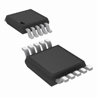
LM5067MM-2/NOPB National Semiconductor, LM5067MM-2/NOPB Datasheet - Page 13

LM5067MM-2/NOPB
Manufacturer Part Number
LM5067MM-2/NOPB
Description
IC CTLR NEG HOTSWAP A/R 10MSOP
Manufacturer
National Semiconductor
Type
Hot-Swap Controllerr
Datasheet
1.LM5067MM-1NOPB.pdf
(24 pages)
Specifications of LM5067MM-2/NOPB
Applications
General Purpose
Internal Switch(s)
No
Voltage - Supply
-9 V ~ -80 V
Operating Temperature
-40°C ~ 125°C
Mounting Type
Surface Mount
Package / Case
10-TFSOP, 10-MSOP (0.118", 3.00mm Width)
For Use With
LM5067EVAL - NEGATIVE HOT SWAP / INRUSH CURRE
Lead Free Status / RoHS Status
Lead free / RoHS Compliant
Other names
LM5067MM-2TR
Available stocks
Company
Part Number
Manufacturer
Quantity
Price
Company:
Part Number:
LM5067MM-2/NOPB
Manufacturer:
TI
Quantity:
4 500
If the system input voltage falls below the UVLO threshold, or
rises above the OVLO threshold, the GATE pin is pulled low
by the 2.2 mA pull-down current to switch off Q1.
Current Limit
The current limit threshold is reached when the voltage across
the sense resistor R
current limiting condition, the GATE voltage is controlled to
limit the current in MOSFET Q1. While the current limit circuit
is active, the fault timer is active as described in the Fault
Timer & Restart section. If the load current reduces below the
current limit threshold before the end of the Fault Timeout
Period, the LM5067 resumes normal operation. For proper
operation, the R
mΩ.
Circuit Breaker
If the load current increases rapidly (e.g., the load is short-
circuited) the current in the sense resistor (R
the current limit threshold before the current limit control loop
is able to respond. If the current exceeds approximately twice
the current limit threshold (100 mV/R
pulled down by the 110 mA pull-down current at the GATE
pin, and a Fault Timeout Period begins. When the voltage
across R
at the GATE pin is switched off, and the gate voltage of Q1 is
then determined by the current limit or the power limit func-
tions. If the TIMER pin reaches 4.0V before the current limiting
or power limiting condition ceases, Q1 is switched off by the
2.2 mA pull-down current at the GATE pin as described in the
Fault Timer & Restart section.
Power Limit
An important feature of the LM5067 is the MOSFET power
limiting. The Power Limit function can be used to maintain the
S
falls below 100 mV the 110 mA pull-down current
S
FIGURE 4. Gate Control
resistor value should be no larger than 100
S
(SENSE to VEE) reaches 50 mV. In the
S
), Q1’s gate is quickly
S
) may exceed
30030931
13
maximum power dissipation of MOSFET Q1 within the device
SOA rating. The LM5067 determines the power dissipation in
Q1 by monitoring its drain-source voltage (OUT to SENSE),
and the drain current through the sense resistor (SENSE to
VEE). The product of the current and voltage is compared to
the power limit threshold programmed by the resistor at the
PWR pin. If the power dissipation reaches the limiting thresh-
old, the GATE voltage is modulated to reduce the current in
Q1, and the fault timer is active as described in the Fault Timer
& Restart section.
Fault Timer & Restart
When the current limit or power limit threshold is reached
during turn-on or as a result of a fault condition, the gate-to-
source voltage of Q1 is modulated to regulate the load current
and power dissipation in Q1. When either limiting function is
active, an 85 µA fault timer current source charges the exter-
nal capacitor (C
(Fault Timeout Period). If the fault condition subsides before
the TIMER pin reaches 4.0V, the LM5067 returns to the nor-
mal operating mode and C
current sink. If the TIMER pin reaches 4.0V during the Fault
Timeout Period, Q1 is switched off by a 2.2 mA pull-down
current at the GATE pin. The subsequent restart procedure
depends on which version of the LM5067 is in use.
The LM5067-1 latches the GATE pin low at the end of the
Fault Timeout Period, and C
current sink. The GATE pin is held low until a power up se-
quence is externally initiated by cycling the input voltage
(V
of VEE with an open-collector or open-drain device as shown
in Figure 5. The voltage across C
restart procedure to be effective.
The LM5067-2 provides an automatic restart sequence which
consists of the TIMER pin cycling between 4.0V and 1.25V
seven times after the Fault Timeout Period, as shown in Fig-
ure 6. The period of each cycle is determined by the 85 µA
charging current, and the 2.5 µA discharge current, and the
value of the capacitor C
during the eighth high-to-low ramp, the 52 µA current source
at the GATE pin turns on Q1. If the fault condition is still
present, the Fault Timeout Period and the restart cycle repeat.
SYS
), or momentarily pulling the UVLO/EN pin within 2.5V
FIGURE 5. Latched Fault Restart Control
T
) at the TIMER pin as shown in Figure 6
T
. When the TIMER pin reaches 0.3V
T
T
is discharged by the 2.5 µA fault
is discharged by the 2.5 µA
T
must be <0.3V for the
www.national.com
30030932


