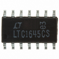
LTC1645CS#PBF Linear Technology, LTC1645CS#PBF Datasheet - Page 9

LTC1645CS#PBF
Manufacturer Part Number
LTC1645CS#PBF
Description
IC CTLR HOT SWAP SEQ DUAL 14SOIC
Manufacturer
Linear Technology
Type
Hot-Swap Controllerr
Datasheet
1.LTC1645CS8PBF.pdf
(24 pages)
Specifications of LTC1645CS#PBF
Applications
General Purpose
Internal Switch(s)
No
Voltage - Supply
1.2 V ~ 12 V
Operating Temperature
0°C ~ 70°C
Mounting Type
Surface Mount
Package / Case
14-SOIC (0.154", 3.90mm Width)
Lead Free Status / RoHS Status
Lead free / RoHS Compliant
Available stocks
Company
Part Number
Manufacturer
Quantity
Price
APPLICATIO S I FOR ATIO
No bulk capacitance is present to slow the rate of rise and
heavily damp the parasitic resonance. Instead, the fast
edge shock excites a resonant circuit formed by a combi-
nation of wiring harness, backplane and circuit board
parasitic inductances and FET capacitance. In theory, the
peak voltage should rise to 2X the input supply, but in
practice the peak can reach 2.5X, owing to the effects of
voltage dependent FET capacitance.
The absolute maximum V
13.2V; any circuit with an input of 5V or greater should be
scrutinized for ringing. A well-bypassed backplane should
not escape suspicion: circuit board trace inductances of as
little as 10nH can produce sufficient ringing to overvoltage
V
Check ringing with a fast storage oscilloscope (such as a
LECROY 9314AL DSO) by attaching coax or a probe to V
CC
.
24V
(a) Undamped V
0V
U
CC
CC n
U
1 s/DIV
Waveform (48" Leads)
potential for the LTC1645 is
12V
W
+
–
1645 F05a
POWER
LEADS
8'
U
Figure 5. Ring Experiment
SCOPE
PROBE
CC
and GND, then repeatedly inserting the circuit board into
the backplane. Figures 5a and 5b show typical results in a
12V application with different V
amplitude reaches 22V, breaking down the ESD protection
diode in the process.
There are two methods for eliminating ringing: clipping
and snubbing. A transient voltage suppressor is an effec-
tive means of limiting peak voltage to a safe level.
Figure 6 shows the effect of adding an ON Semiconductor,
1SMA12CAT3, on the waveform of Figure 5.
Figures 7a and 7b show the effects of snubbing with
different RC networks. The capacitor value is chosen as
10X to 100X the FET C
best damping—1
parasitic inductance.
0.01
LTC1645
R1
IRF7413
24V
0V
(b) Undamped V
10
1645 F05
+
0.1 F
C
LOAD
V
to 50
OUT
OSS
CC
1 s/DIV
under bias and R is selected for
Waveform (8" Leads)
depending on the value of
CC
lead lengths. The peak
1645 F05b
LTC1645
1645fa
9


