LTC4268IDKD-1#PBF Linear Technology, LTC4268IDKD-1#PBF Datasheet
LTC4268IDKD-1#PBF
Specifications of LTC4268IDKD-1#PBF
Available stocks


Related parts for LTC4268IDKD-1#PBF


LTC4268IDKD-1#PBF Summary of contents
Page 1
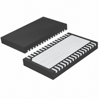
... The LTC4268-1 is available in a space saving 32-pin DFN package. L, LT, LTC and LTM are registered trademarks of Linear Technology Corporation. All other trademarks are the property of their respective owners. Protected by U.S. Patents including 5841643. 35W High Effi ciency PD Solution ...
Page 2
... LTC4268-1I .......................................... –40°C to 85°C Junction Temperature (Note 5) ............................. 150°C Storage Temperature Range ................... –65°C to 150°C ORDER INFORMATION LEAD FREE FINISH TAPE AND REEL LTC4268CDKD-1#PBF LTC4268CDKD-1#TRPBF LTC4268IDKD-1#PBF LTC4268IDKD-1#TRPBF LEAD BASED FINISH TAPE AND REEL LTC4268CDKD-1 LTC4268CDKD-1#TR LTC4268IDKD-1 LTC4268IDKD-1#TR Consult LTC Marketing for parts specifi ed with wider operating temperature ranges. *The temperature grade is identifi label on the shipping container. ...
Page 3
ELECTRICAL CHARACTERISTICS temperature range, otherwise specifi cations are 27.4k 90k, unless otherwise specifi ed. PGDLY ENDLY SYMBOL PARAMETER V Supply Voltage PORT IEEE 802.3af System Signature Range Classifi cation Range UVLO Turn-On Voltage UVLO ...
Page 4
LTC4268-1 ELECTRICAL CHARACTERISTICS temperature range, otherwise specifi cations are 27.4k 90k, unless otherwise specifi ed. PGDLY ENDLY SYMBOL PARAMETER R Shutdown Input Resistance INPUT_SHDN V I High Level Input Voltage IH_ILIM LIM_EN V I ...
Page 5
ELECTRICAL CHARACTERISTICS temperature range, otherwise specifi cations are 27.4k 90k, unless otherwise specifi ed. PGDLY ENDLY SYMBOL PARAMETER I Feedback Pin Load Compensation LCOMP Current V Load Comp to V Offset Voltage LCOMP SENSE ...
Page 6
LTC4268-1 TYPICAL PERFORMANCE CHARACTERISTICS Input Current vs Input Voltage 25k Detection Range 0 25°C A 0.4 0.3 0.2 0 –2 –4 –6 –8 INPUT VOLTAGE (V) 42681 G01 Signature Resistance vs Input Voltage ...
Page 7
TYPICAL PERFORMANCE CHARACTERISTICS V and V CC(ON) CC(OFF) vs Temperature CC(ON CC(OFF –50 – 100 TEMPERATURE (°C) 42681 G10 SENSE Voltage vs Temperature 110 FB ...
Page 8
LTC4268-1 TYPICAL PERFORMANCE CHARACTERISTICS Feedback Amplifi er Output Current 125°C 25°C 50 –40° –10 –30 –50 –70 0.9 1 1.1 1.2 1.3 1.4 V (V) FB 42681 G19 Feedback Amplifi er Voltage Gain vs ...
Page 9
TYPICAL PERFORMANCE CHARACTERISTICS Minimum PG On Time vs Temperature 340 R = 158k tON(MIN) 330 320 310 300 290 280 270 260 –50 – 100 TEMPERATURE (°C) 42681 G28 PIN FUNCTIONS SHDN (Pin 1): Shutdown Input. ...
Page 10
LTC4268-1 PIN FUNCTIONS SFST (Pin 14): Soft-Start. This pin, in conjunction with a capacitor ( GND, controls the ramp-up of peak SFST primary current through the sense resistor also used to control converter inrush at start-up. ...
Page 11
PIN FUNCTIONS PGDLY (Pin 23): Primary Gate Delay Control. Connect an external programming resistor (R PGDLY synchronous gate turn-off to primary gate turn-on. See Applications Information for details. PG (Pin 24): Primary Gate Drive the gate drive pin ...
Page 12
LTC4268-1 BLOCK DIAGRAM SHDN CLASS 3 I LIM_EN 4 V PORTN 5 V PORTN 6 V PORTN 7 V UVLO CC + – 1.237V 15.3V REFERENCE (V UVLO 18 OSC 15 OSCILLATOR SYNC ...
Page 13
... LTC4268-1 to allow quick implementation of a custom system. Alternately, the system vendor can choose to build their own high power PSE. Linear Technology provides complete application information for high power PSE solutions delivering up to 35W for 2-pair systems and as much as 70W when used in 4-pair systems ...
Page 14
LTC4268-1 APPLICATIONS INFORMATION The LTC4268-1 is specifi cally designed to implement the high power PD front end and switching regulator for power-hungry PoE applications that must operate beyond the power limits of IEEE 802.3af. The LTC4268-1 uses a precision, dual ...
Page 15
APPLICATIONS INFORMATION OPERATION Note: Please refer to the simplifi ed application circuit (Figure 2) for voltage naming conventions used in this datasheet. The LTC4268-1 high power PD interface controller and switching regulator has several modes of operation depend- ing on ...
Page 16
LTC4268-1 APPLICATIONS INFORMATION The IEEE 802.3af specifi cation requires the PSE to use a ΔV/ΔI measurement technique to keep the DC offset voltage of the diode bridge from affecting the signature resistance measurement. However, the diode resistance appears in series ...
Page 17
APPLICATIONS INFORMATION In some designs that include an auxiliary power option, such as an external wall adapter necessary to control whether or not the PD is detected by a PSE. With the LTC4268-1, the 25k signature resistor can ...
Page 18
LTC4268-1 APPLICATIONS INFORMATION defi ned here is available for system vendors to implement a unique classifi cation for use in closed systems and is not defi ned or supported by the IEEE 802.3af. With the extended classifi cation range available ...
Page 19
APPLICATIONS INFORMATION UNDERVOLTAGE LOCKOUT The IEEE 802.3af specifi cation dictates a maximum turn-on voltage of 42V and a minimum turn-off voltage of 30V for the PD. In addition, the PD must maintain large on-off hysteresis to prevent current-resistance (I-R) drops ...
Page 20
LTC4268-1 APPLICATIONS INFORMATION During the inrush event being charged, a large amount of power is dissipated in the MOSFET. The LTC4268-1 is designed to accept this load and is thermally protected to avoid damage to the onboard ...
Page 21
APPLICATIONS INFORMATION The active high PWRGD pin features an internal, open-collector output referenced to V the active high PWRGD pin becomes valid when C1 reaches –4V and pulls low until the load capacitor is fully charged. At that point, PWRGD ...
Page 22
LTC4268-1 APPLICATIONS INFORMATION nuisance trips of the thermal shutdown, it may be necessary to limit the maximum ambient temperature. Limiting the die temperature to 125°C will keep the LTC4268-1 from hitting thermal shutdown. For DC loads the maximum ambient temperature ...
Page 23
APPLICATIONS INFORMATION isolation transformer and proper termination methods. These vendors have transformers specifi cally designed for use in high power PD applications. IEEE 802.3af allows power wiring in either of two confi gurations on the TX/RX wires, and power can ...
Page 24
LTC4268-1 APPLICATIONS INFORMATION OPTION 1: AUXILIARY POWER INSERTED BEFORE LTC4268-1 RJ45 + – PHY 3 – SPARE – SPARE 8 + ISOLATED WALL V WW TRANSFORMER ...
Page 25
APPLICATIONS INFORMATION It is necessary to include diode D9 to prevent the adapter from applying power to the LTC4268-1. Power priority issues require more intervention. If the adapter voltage is below the PSE voltage, then the priority will be given ...
Page 26
LTC4268-1 APPLICATIONS INFORMATION I is the LTC4268-1 IC supply current during IN_CLASS classifi cation given in the electrical specifi cations. The R resistor must better to avoid degrading CLASS the overall accuracy of the classifi cation circuit. ...
Page 27
... IEEE 802.3at Interoperability In anticipation of the IEEE 802.3at standard release, the LTC4268-1 can be combined with a simple external circuit to be fully interoperable with an IEEE 802.3at-compliant PSE. For more information, please contact Linear Technology’s Application Engineering. ACTIVE-HIGH ENABLE V PORTP ...
Page 28
LTC4268-1 APPLICATIONS INFORMATION The fl yback voltage is scaled by an external resistive divider R1/R2 and presented at the FB pin. The feedback amplifi er compares the voltage to the internal bandgap reference. The feedback amp is actually a transconductance ...
Page 29
APPLICATIONS INFORMATION Combining this with the previous V FLBK an expression for V in terms of the internal reference, OUT programming resistors and secondary resistances: ⎛ ⎞ R1 −I V • V • N ⎝ ⎜ ⎠ ⎟ ...
Page 30
LTC4268-1 APPLICATIONS INFORMATION source is caused by transformer secondary current fl ow through the synchronous MOSFET R nonzero impedances of the transformer secondary and output capacitor. This was represented previously by the expression “I • (ESR + R ).” However, ...
Page 31
APPLICATIONS INFORMATION where dimensionless variable related and effi ciency as explained above OUT R = external sense resistor SENSE Nominal output impedance cancellation is obtained by equating this expression with R S(OUT) ESR + R ...
Page 32
LTC4268-1 APPLICATIONS INFORMATION Leakage Inductance Transformer leakage inductance (on either the primary or secondary) causes a spike after the primary side switch turn-off. This is increasingly prominent at higher load currents, where more stored energy is dissipated. Higher fl yback ...
Page 33
APPLICATIONS INFORMATION Winding Resistance Effects Primary or secondary winding resistance acts to reduce overall effi ciency ( Secondary winding resistance OUT IN increases effective output impedance, degrading load regu- lation. Load compensation can mitigate this to some extent ...
Page 34
LTC4268-1 APPLICATIONS INFORMATION The main design goals for core selection are reducing copper losses and preventing saturation. Ferrite core material saturates hard, rapidly reducing inductance when the peak design current is exceeded. This results in an abrupt increase in inductor ...
Page 35
APPLICATIONS INFORMATION assume that our worst-case conditions yield an I above nominal 2.3A. If there is a 10% tolerance and minimum V = 88mV, then R SENSE SENSE 110% = 88mV/2.3A and nominal R ...
Page 36
LTC4268-1 APPLICATIONS INFORMATION Setting Frequency The switching frequency of the LTC4268-1 is set by an external capacitor connected between the OSC pin and ground. Recommended values are between 200pF and 33pF , yielding switching frequencies between 50kHz and 250kHz. Figure ...
Page 37
APPLICATIONS INFORMATION the actual secondary output voltage. The enable delay time should be made long enough to ignore the “irrelevant” portion of the fl yback waveform at light loads. Even though the LTC4268-1 has a robust gate drive, the gate ...
Page 38
LTC4268-1 APPLICATIONS INFORMATION V CMP 17 C VCMP2 42681 F16 Figure 16. V Compensation Network CMP In operation, the “trickle charge” resistor and supplies a small current, typically on the order IN of 1mA to charge C ...
Page 39
APPLICATIONS INFORMATION Slope Compensation The LTC4268-1 incorporates current slope compensation. Slope compensation is required to ensure current loop stability when the DC is greater than 50%. In some switching regulators, slope compensation reduces the maximum peak current at higher duty ...
Page 40
LTC4268-1 APPLICATIONS INFORMATION MILLER EFFECT GATE CHARGE ( Figure 17. Gate Charge Curve • The external feedback resistive divider ratio directly affects regulated voltage. Use 1% components. • Leakage inductance ...
Page 41
APPLICATIONS INFORMATION For each secondary-side power MOSFET RMS current is given by: I OUT = I RMS(SEC) 1− DC MAX Calculate MOSFET power dissipation next. Because the primary-side power MOSFET operates at high V transition power loss term is included ...
Page 42
LTC4268-1 APPLICATIONS INFORMATION I PRI PRIMARY CURRENT SECONDARY CURRENT ΔV COUT OUTPUT VOLTAGE RIPPLE WAVEFORM ΔV ESR Figure 18. Typical Flyback Converter Waveforms However, other schemes are possible. There are gate drivers and secondary side synchronous controllers available that provide ...
Page 43
... LTC4268- highly recommended that the SMAJ58A unidirectional 58V transient voltage suppressor be installed between the diode bridge and the LTC4268-1 (D3 in Figure 4). SwitcherCAD is a trademark of Linear Technology Corporation. LTC4268-1 1/4 the size of the nonfi lter OUT to make the second fi lter OUT ...
Page 44
LTC4268-1 APPLICATIONS INFORMATION ISOLATION The 802.3 standard requires Ethernet ports to be electrically isolated from all other conductors that are user accessible. This includes the metal chassis, other connectors and any auxiliary power connection. For PDs, there are two common ...
Page 45
APPLICATIONS INFORMATION VCC • • GATE TURN- VIN GATE TURN-OFF R SENSE + GATE C R TURN- • • GATE Q3 ...
Page 46
LTC4268-1 TYPICAL APPLICATION 46 42681fb ...
Page 47
... ALL DIMENSIONS ARE IN MILLIMETERS Information furnished by Linear Technology Corporation is believed to be accurate and reliable. However, no responsibility is assumed for its use. Linear Technology Corporation makes no representa- tion that the interconnection of its circuits as described herein will not infringe on existing patent rights. DKD Package 32-Lead Plastic DFN (7mm × ...
Page 48
... High Power PD Interface Controller With 750mA Current Limit LTC4267 IEEE 802.3af PD Interface With an Integrated Switching Regulator LTC4267-3 IEEE 802.3af PD Interface With an Integrated Switching Regulator ThinSOT is a trademark of Linear Technology Corporation. 48 Linear Technology Corporation 1630 McCarthy Blvd., Milpitas, CA 95035-7417 (408) 432-1900 FAX: (408) 434-0507 ● COMMENTS ...