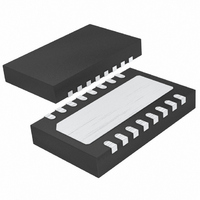
LTC4218CDHC-12#PBF Linear Technology, LTC4218CDHC-12#PBF Datasheet

LTC4218CDHC-12#PBF
Specifications of LTC4218CDHC-12#PBF
Available stocks
Related parts for LTC4218CDHC-12#PBF
LTC4218CDHC-12#PBF Summary of contents
Page 1
... Overvoltage, undervoltage and power good monitoring are also provided. L, LT, LTC, LTM, Linear Technology and the Linear logo are registered trademarks and Hot Swap is a trademark of Linear Technology Corporation. All other trademarks are the property of their respective owners. V OUT ...
Page 2
... T = 43°C/W JMAX JA EXPOSED PAD (PIN 17) IS SUBSTRATE GND ORDER INFORMATION LEAD FREE FINISH TAPE AND REEL LTC4218CDHC-12#PBF LTC4218CDHC-12#TRPBF LTC4218IDHC-12#PBF LTC4218IDHC-12#TRPBF LTC4218CGN#PBF LTC4218CGN#TRPBF LTC4218IGN#PBF LTC4218IGN#TRPBF Consult LTC Marketing for parts specifi ed with wider operating temperature ranges. *The temperature grade is identifi label on the shipping container. ...
Page 3
ELECTRICAL CHARACTERISTICS temperature range, otherwise specifi cations are at T SYMBOL PARAMETER DC Characteristics V Input Supply Range DD I Input Supply Current DD V Input Supply Undervoltage Lockout DD(UVL) V Input Supply Undervoltage Threshold DD(UVTH) ΔV Input Supply Undervoltage ...
Page 4
LTC4218 ELECTRICAL CHARACTERISTICS temperature range, otherwise specifi cations are at T SYMBOL PARAMETER I TIMER Pin Current Ratio I TIMER(RATIO) I TIMER(UP Full-Scale Output Current MON(FS) MON I I Pin Offset Current MON(OFF) MON G I Pin Gain ...
Page 5
TYPICAL PERFORMANCE CHARACTERISTICS 2.0 1.8 85°C 1.6 25°C 1.4 –40°C 1.2 1 (V) DD 4218 G01 UV Hysteresis vs Temperature 0.10 0.08 0.06 0.04 –50 – ...
Page 6
LTC4218 TYPICAL PERFORMANCE CHARACTERISTICS GATE Pull-Up Current vs Temperature –26.0 –25.5 –25.0 –24.5 –24.0 –50 – TEMPERATURE (°C) 4218 G10 Gate Drive vs Temperature 6.15 6.14 6.13 6.12 6.11 6.10 –50 – ...
Page 7
PIN FUNCTIONS Exposed Pad: Exposed pad may be left open or connected to device ground. FB: Foldback and Power Good Comparator Input. Connect this pin to an external resistive divider from SOURCE for the LTC4218 (adjustable version). The LTC4218-12 version ...
Page 8
LTC4218 FUNCTIONAL DIAGRAM + SENSE V DD +– 1.235V 140k – 20k * + 0.62V RST – 224k * OV + 20k OV * – 1.235V – UVLO1 + 2.73V ...
Page 9
OPERATION The Functional Diagram displays the main circuits of the device. The LTC4218 is designed to turn a board’s sup- ply voltage on and off in a controlled manner, allowing the board to be safely inserted and removed from a ...
Page 10
LTC4218 APPLICATIONS INFORMATION The typical LTC4218 application high availability system that uses a positive voltage supply to distribute power to individual cards. The basic application circuit is shown in Figure 1. External component selection is discussed in ...
Page 11
APPLICATIONS INFORMATION If V drops below 2.65V for greater than 5μs or INTV DD drops below 2.5V for greater than 1μs, a fast shutdown of the switch is initiated. The GATE is pulled down with a 170mA current to the ...
Page 12
LTC4218 APPLICATIONS INFORMATION Monitor MOSFET Current The current in the MOSFET passes through the sense resistor. The voltage on the sense resistor is converted to a current that is sourced out of the I the I amplifi 100μA ...
Page 13
APPLICATIONS INFORMATION In this same fi gure the OV threshold is lowered from 15.05V to 13.5V. Decreasing the OV threshold requires adding a resistor between V and OV. This resistor can DD be calculated as follows: ( ⎛ ...
Page 14
LTC4218 APPLICATIONS INFORMATION Next, the power dissipated in the MOSFET during overcur- rent must be limited. The active current limit uses a timer to prevent excessive energy dissipation in the MOSFET. The worst-case power occurs when the voltage versus current ...
Page 15
APPLICATIONS INFORMATION It is also important to put C1, the bypass capacitor for the INTV pin, as close as possible between the INTV CC GND. Place the 10Ω resistor as close as possible to Q1. This will limit the parasitic ...
Page 16
LTC4218 PACKAGE DESCRIPTION 3.50 ±0.05 1.65 ±0.05 2.20 ±0.05 (2 SIDES) 0.25 ± 0.05 0.50 BSC 4.40 ±0.05 (2 SIDES) RECOMMENDED SOLDER PAD PITCH AND DIMENSIONS NOTE: 1. DRAWING PROPOSED TO BE MADE VARIATION OF VERSION (WJED-1) IN JEDEC PACKAGE ...
Page 17
... Revised Additional Applications section and inserted Figure 8 in Applications Information. Information furnished by Linear Technology Corporation is believed to be accurate and reliable. However, no responsibility is assumed for its use. Linear Technology Corporation makes no representa- tion that the interconnection of its circuits as described herein will not infringe on existing patent rights. ...
Page 18
... CompactPCI, or 3.3V, 3.3V Auxiliary and 12V for PCI- Express, Monitors Voltage and Current with 8-Bit ADC www.linear.com ● V OUT 24V 6A + 158k 330μF 1k 0.01μF 10k 24V 10k ADC 20k 4218 TA02 LT 0410 REV E • PRINTED IN USA © LINEAR TECHNOLOGY CORPORATION 2007 4218fe ...


