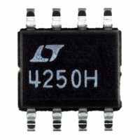
LT4250HCS8#PBF Linear Technology, LT4250HCS8#PBF Datasheet - Page 5

LT4250HCS8#PBF
Manufacturer Part Number
LT4250HCS8#PBF
Description
IC CONTRLR HOTSWAP NEG 48V 8SOIC
Manufacturer
Linear Technology
Type
Hot-Swap Controllerr
Datasheet
1.LT4250HCS8PBF.pdf
(14 pages)
Specifications of LT4250HCS8#PBF
Applications
General Purpose
Internal Switch(s)
No
Voltage - Supply
-20 V ~ -80 V
Operating Temperature
0°C ~ 70°C
Mounting Type
Surface Mount
Package / Case
8-SOIC (0.154", 3.90mm Width)
Output Voltage
1.2V
Internal Switch
No
Supply Voltage Range
18V To 80V
Digital Ic Case Style
SOIC
No. Of Pins
8
Operating Temperature Range
0°C To +70°C
Msl
MSL 1 - Unlimited
Rohs Compliant
Yes
Lead Free Status / RoHS Status
Lead free / RoHS Compliant
Available stocks
Company
Part Number
Manufacturer
Quantity
Price
PIN FUNCTIONS
PWRGD/PWRGD (Pin 1): Power Good Output Pin. This pin
will latch a power good indication when V
V
can be connected directly to the enable pin of a power
module.
When the DRAIN pin of the LT4250L is above V
than V
PWRGD pin will be high impedance, allowing the pull-up
current of the module’s enable pin to pull the pin high and
turn the module off. When V
V
V
This condition is latched until the GATE pin is turned off
via the UV, OV, UVLO or the electronic circuit breaker.
When the DRAIN pin of the LT4250H is above V
than V
PWRGD pin will sink current to the DRAIN pin which pulls
the module’s enable pin low, forcing it off. When V
drops below V
sink current is turned off, allowing the module’s pull-up
current to pull the enable pin high and turn on the module.
This condition is latched until the GATE pin is turned off
via the UV, OV, UVLO or the electronic circuit breaker.
OV (Pin 2): Analog Overvoltage Input. When OV is pulled
above the 1.255V threshold, an overvoltage condition is
detected and the GATE pin will be immediately pulled low.
The GATE pin will remain low until OV drops below the
1.235V threshold.
UV (Pin 3): Analog Undervoltage Input. When UV is pulled
below the 1.125V threshold, an undervoltage condition
is detected and the GATE pin will be immediately pulled
low. The GATE pin will remain low until UV rises above
the 1.255 threshold.
The UV pin is also used to reset the electronic circuit
breaker. If the UV pin is cycled low and high following the
trip of the circuit breaker, the circuit breaker is reset and a
normal power-up sequence will occur. The response time
DL
GATE
EE
, pulling the enable pin low and turning on the module.
of V
rises above V
DL
DL
EE
or V
or V
and V
DL
GATE
GATE
and V
GATE
is more than V
is more than V
GH
is within V
, the PWRGD pin sinks current to
GATE
rises above V
DRAIN
GH
drops below V
GH
GH
of ΔV
from ΔV
from ΔV
GH
DRAIN
GATE
, the PWRGD
EE
EE
. This pin
GATE
GATE
is within
by more
by more
DL
DRAIN
, the
, the
and
for this pin is 1.5μs. Add an external capacitor to this pin
for additional filtering.
V
the lower potential of the power supply.
SENSE (Pin 5): Circuit Breaker Sense Pin. With a sense
resistor placed in the supply path between V
the overcurrent condition will pull down the GATE pin and
regulate the voltage across the resistor to be 50mV. If
the overcurrent condition exists for more than 500μs the
electronic circuit breaker will trip and turnoff the external
MOSFET.
If the current limit value is set to twice the normal operating
current, only 25mV is dropped across the sense resistor
during normal operation. To disable the current limit feature,
V
GATE (Pin 6): Gate Drive Output for the External N-channel
MOSFET. The GATE pin will go high when the following
start-up conditions are met: the UV pin is high, the OV pin
is low, (V
than V
rent source and pulled low with a 50mA current source.
During current limit the GATE pin is pulled low using a
100mA current source.
DRAIN (Pin 7): Analog Drain Sense Input. Connect this
pin to the drain of the external N-channel MOSFET and
the V
below V
the switch is on.
V
pin to the higher potential of the power supply inputs and
the V
circuit disables the chip until the V
the 16V V
EE
EE
DD
and SENSE can be shorted together.
(Pin 4): Negative Supply Voltage Input. Connect to
(Pin 8): Positive Supply Voltage Input. Connect this
+
–
UVLOH
pin of the power module. An undervoltage lockout
pin of the power module. When the DRAIN pin is
DL
SENSE
UVLOH
, the PWRGD/PWRGD pin will latch to indicate
. The GATE pin is pulled high by a 45μA cur-
– V
threshold.
EE
) < 50mV and the V
LT4250L/LT4250H
DD
pin is greater than
DD
EE
pin is greater
and SENSE,
4250lhfa
5


