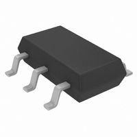
LTC4210-1IS6#TRMPBF Linear Technology, LTC4210-1IS6#TRMPBF Datasheet - Page 8

LTC4210-1IS6#TRMPBF
Manufacturer Part Number
LTC4210-1IS6#TRMPBF
Description
IC CONTROLLER HOT SWAP TSOT23-6
Manufacturer
Linear Technology
Type
Hot-Swap Controllerr
Datasheet
1.LTC4210-1CS6TRMPBF.pdf
(20 pages)
Specifications of LTC4210-1IS6#TRMPBF
Applications
General Purpose
Internal Switch(s)
No
Voltage - Supply
2.7 V ~ 16.5 V
Operating Temperature
-40°C ~ 85°C
Mounting Type
Surface Mount
Package / Case
SOT-23-6 Thin, TSOT-23-6
Input Voltage
17V
Output Voltage
3V
Internal Switch
No
Rohs Compliant
Yes
Lead Free Status / RoHS Status
Lead free / RoHS Compliant
Other names
LTC4210-1IS6#TRMPBFTR
Available stocks
Company
Part Number
Manufacturer
Quantity
Price
LTC4210-1/LTC4210-2
APPLICATIO S I FOR ATIO
Hot Circuit Insertion
When circuit boards are inserted into live backplanes, the
supply bypass capacitors can draw large transient cur-
rents from the backplane power bus as they charge. Such
transient currents can cause permanent damage to con-
nector pins, glitches on the system supply or reset other
boards in the system.
The LTC4210 is designed to turn a printed circuit board’s
supply voltage ON and OFF in a controlled manner, allow-
ing the circuit board to be safely inserted into or removed
from a live backplane. The LTC4210 can reside either on
the backplane or on the daughter board for hot circuit
insertion applications.
Overview
The LTC4210 is designed to operate over a range of
supplies from 2.7V to 16.5V. Upon insertion, an undervolt-
age lockout circuit determines if sufficient supply voltage
is present. When the ON pin goes high an initial timing
cycle assures that the board is fully seated in the backplane
before the MOSFET is turned on. A single timer capacitor
sets the periods for all of the timer functions. After the
initial timing cycle the LTC4210 can either start up in
current limit or with a lower load current. Once the external
MOSFET is fully enhanced and the supply has ramped up,
the LTC4210 monitors the load current through an exter-
nal sense resistor. Overcurrent faults are actively limited
to 50mV/R
The LTC4210-1 will automatically retry after a current limit
fault while the LTC4210-2 latches off. The LTC4210-1
timer function limits the retry duty cycle to 3.8% for
MOSFET cooling.
Undervoltage Lockout
An internal undervoltage lockout (UVLO) circuit resets the
LTC4210 if the V
8
SENSE
CC
for a specified circuit breaker timer limit.
supply is too low for normal operation.
U
U
W
U
The UVLO has a low-to-high threshold of 2.5V, a 100mV
hysteresis and a high-to-low glitch filter of 30 s. Above
2.5V supply voltage, the LTC4210 will start if the ON pin
conditions are met. A short supply dip below 2.4V for less
than 30 s is ignored to allow for bus supply transients.
ON Function
The ON pin is the input to a comparator which has a low-
to-high threshold of 1.3V, an 80mV hysteresis and a high-
to-low glitch filter of 30 s. A low input on the ON pin resets
the LTC4210 TIMER status and turns off the external
MOSFET by pulling the GATE pin to ground. A low-to-high
transition on the ON pin starts an initial cycle followed by
a start-up cycle. A 10k pull-up resistor connecting the ON
pin to the supply is recommended. The 10k resistor shunts
any potential static charge on the backplane and reduces
the overvoltage stress at the ON pin during live insertion.
Alternatively, an external resistor divider at the ON pin can
be used to program an undervoltage lockout value higher
than the internal UVLO circuit. An RC filter can be added at
the ON pin to increase the delay time at card insertion if the
internal glitch filter delay is insufficient.
GATE Function
During hot insertion of the PCB, an abrupt application of
supply voltage charges the external MOSFET drain/gate
capacitance. This can cause an unwanted gate voltage
spike. An internal proprietary circuit holds GATE low
before the internal circuitry wakes up. This reduces the
MOSFET current surges substantially at insertion. The
GATE pin is held low in reset mode and during the initial
timing cycle. In the start-up cycle the GATE pin is pulled up
by a 10 A current source. During an overcurrent fault
condition, the error amplifier servoes the GATE pin to
maintain a constant current to the load until the circuit
breaker trips. When the circuit breaker trips, the GATE pin
shuts down abruptly.
421012f


