MCP3909-I/SS Microchip Technology, MCP3909-I/SS Datasheet - Page 15
MCP3909-I/SS
Manufacturer Part Number
MCP3909-I/SS
Description
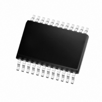
IC POWER METERING-1 PHASE 24SSOP
Manufacturer
Microchip Technology
Datasheets
1.MCP3909T-ISS.pdf
(44 pages)
2.MCP3909T-ISS.pdf
(104 pages)
3.MCP3909-ISS.pdf
(40 pages)
Specifications of MCP3909-I/SS
Package / Case
24-SSOP (0.200", 5.30mm Width)
Input Impedance
390 KOhm
Measurement Error
0.1%
Voltage - I/o High
2.4V
Voltage - I/o Low
0.85V
Current - Supply
2.3mA
Voltage - Supply
4.5 V ~ 5.5 V
Operating Temperature
-40°C ~ 85°C
Mounting Type
Surface Mount
Meter Type
Single Phase
Operating Temperature Range
- 40 C to + 85 C
Mounting Style
SMD/SMT
Supply Voltage Range
4.5V To 5.5V
Digital Ic Case Style
SSOP
No. Of Pins
24
Interface Type
Serial, SPI
Supply Voltage Max
5.5V
Rohs Compliant
Yes
Lead Free Status / RoHS Status
Lead free / RoHS Compliant
For Use With
MCP3909EV-MCU16 - EVALUATION BOARD FOR MCP3909MCP3909RD-3PH1 - REF DESIGN MCP3909 3PH ENGY MTR
Lead Free Status / Rohs Status
Lead free / RoHS Compliant
Available stocks
Company
Part Number
Manufacturer
Quantity
Price

Part Number:
MCP3909-I/SS
Manufacturer:
MICROCHIP/微芯
Quantity:
20 000


3.0
The descriptions of the pins are listed in
TABLE 3-1:
3.1
DV
within the MCP3909.
This pin requires appropriate bypass capacitors and
should be maintained to 5V ±10% for specified
operation.
Information”.
3.2
HPF controls the state of the high-pass filter in both
input channels. A logic ‘1’ enables both filters,
removing any DC offset coming from the system or the
device. A logic ‘0’ disables both filters allowing DC
voltages to be measured.
© 2009 Microchip Technology Inc.
DD
MCP3909
is the power supply pin for the digital circuitry
SSOP
PIN DESCRIPTIONS
Digital V
High-Pass Filter Input Logic Pin
(HPF)
10
11
12
13
14
15
16
17
18
19
20
21
22
23
24
1
2
3
4
5
6
7
8
9
Refer
PIN FUNCTION TABLE
DD
to
(DV
REFIN/OUT
SDO / NEG
Section 6.0
SCK / F2
SDI / F1
Symbol
CS / F0
HF
MCLR
OSC1
OSC2
F
F
CH0+
CH1+
DV
A
D
AV
CH0-
CH1-
HPF
DD
OUT1
OUT0
NC
NC
G1
G0
GND
GND
OUT
DD
DD
)
“Applications
Table
Digital Power Supply Pin
High-Pass Filters Control Logic Pin
Analog Power Supply Pin
No Connect
Master Clear Logic Input Pin
Analog Ground Pin, Return Path for internal analog circuitry
Serial Clock or Frequency Control for HF
Serial Data Input or Frequency Control for F
Chip Select or Frequency Control for F
Gain Control Logic Input Pin
Gain Control Logic Input Pin
Oscillator Crystal Connection Pin or Clock Input Pin
Oscillator Crystal Connection Pin or Clock Output Pin
No Connect
Serial Data Out or Negative Power Logic Output Pin
Digital Ground Pin, Return Path for Internal Digital Circuitry
High-Frequency Logic Output Pin (Intended for Calibration)
Differential Mechanical Counter Logic Output Pin
Differential Mechanical Counter Logic Output Pin
Non-Inverting Analog Input Pin for Channel 0 (Current Channel)
Inverting Analog Input Pin for Channel 0 (Current Channel)
Inverting Analog Input Pin for Channel 1 (Voltage Channel)
Non-Inverting Analog Input Pin for Channel 1 (Voltage Channel)
Voltage Reference Input/Output Pin
3-1.
3.3
AV
within the MCP3909.
This pin requires appropriate bypass capacitors and
should be maintained to 5V ±10% for specified
operation.
Information”.
DD
is the power supply pin for the analog circuitry
Analog V
Description
Refer
OUT0/1
OUT
to
OUT0/1
DD
Logic Input Pin
Logic Input Pin
(AV
Section 6.0
Logic Input Pin
DD
MCP3909
)
DS22025B-page 15
“Applications
Related parts for MCP3909-I/SS
Image
Part Number
Description
Manufacturer
Datasheet
Request
R

Part Number:
Description:
Energy Metering IC with SPI Interface and Active Power Pulse Output
Manufacturer:
Microchip Technology
Datasheet:
Part Number:
Description:
Power Meter with SPI and Active Power Pulse Output & Internal Oscillator., -40C to +85C, 28-SPDIP, TUBE
Manufacturer:
Microchip Technology
Datasheet:
Part Number:
Description:
Analog to Digital Converters - ADC Energy Meter IC Gain Dynamic Range
Manufacturer:
Microchip Technology

Part Number:
Description:
Manufacturer:
Microchip Technology Inc.
Datasheet:
Part Number:
Description:
Manufacturer:
Microchip Technology Inc.
Datasheet:
Part Number:
Description:
Manufacturer:
Microchip Technology Inc.
Datasheet:
Part Number:
Description:
Manufacturer:
Microchip Technology Inc.
Datasheet:
Part Number:
Description:
Manufacturer:
Microchip Technology Inc.
Datasheet:
Part Number:
Description:
Manufacturer:
Microchip Technology Inc.
Datasheet:
Part Number:
Description:
Manufacturer:
Microchip Technology Inc.
Datasheet: