MM58248N National Semiconductor, MM58248N Datasheet - Page 3
MM58248N
Manufacturer Part Number
MM58248N
Description
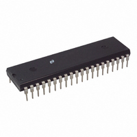
IC DISPLAY DRIVER HI VOLT 40-DIP
Manufacturer
National Semiconductor
Datasheet
1.MM58248N.pdf
(6 pages)
Specifications of MM58248N
Display Type
Vacuum Fluorescent (VF)
Configuration
Alphanumeric or Dot Matrix
Interface
Serial
Current - Supply
150µA
Voltage - Supply
4.5 V ~ 5.5 V
Operating Temperature
-40°C ~ 85°C
Mounting Type
Through Hole
Package / Case
40-DIP (0.600", 15.24mm)
Lead Free Status / RoHS Status
Contains lead / RoHS non-compliant
Digits Or Characters
-
Other names
*MM58248N


Figure 2 shows the pinout of the MM58248 device where
ures 3a and 3b show that this output impedance will remain
Figure 4 demonstrates the critical timing requirements be-
Connection Diagrams
Functional Description
This product is specifically designed to drive multiplexed or
non-multiplexed high voltage alphanumeric or dot matrix
vacuum fluorescent (VF) displays Character generation is
done externally in the microprocessor with a serial data
path to the display driver The MM58248 uses two signals
DATA IN and CLOCK with a format of a leading ‘1’ followed
by the 35 data bits hence allowing data transfer without an
additional signal A block diagram of the MM58248 is shown
in Figure 1
output 1 (pin 18) is equivalent to bit 1 i e the first bit of data
to be loaded into the shift register following the start bit A
logic ‘1’ at the input will turn on the corresponding display
digit segment dot output
A significant reduction in discrete board components can be
achieved by the use of the MM58248 because external
pull-down resistors are not required Due to the nature of
the output stage both its on and off impedance values vary
as a function of the display voltage applied However Fig-
constant for a fixed value of display voltage
tween CLOCK and DATA IN for the MM58248
See NS Package Number N40A
Order Number MM58248N
Dual-In-Line Package
Top View
TL F 5599 – 2
FIGURE 2
3
Figure 6 shows a schematic diagram of a microprocessor-
In Figure 5 a start bit of logic ‘1’ precedes the 35 bits of
data each bit being accepted on the rising edge of CLOCK
i e a ‘0’– ‘1’ transition At the 36th clock a LOAD signal is
generated synchronously with the high state of the clock
thus loading the 35 bits of the shift register into the latches
At the low state of the clock a RESET signal is generated
clearing all bits of the shift register for the next set of data
Hence a complete set of 36 clock pulses is needed for the
MM58248 or the shift register will not clear To clear (reset)
the display driver at ‘power on’ or any time the following
flushing routine may be used Clock in 36 ‘‘zeroes’’ fol-
lowed by a ‘‘one’’ (start bit) followed by 35 ‘‘zeroes’’ This
procedure will completely blank the display It is recom-
mended to clear the driver at power on
based system where the MM58248 is used to provide the
anode drive for a 32-digit 5 x 7 dot matrix vacuum fluores-
cent (VF) display The grid drive in this example is provided
by another member of the high voltage display driver family
namely the MM58241 which has the additional features of
a BLANKING CONTROL pin a DATA OUT pin and an
ENABLE (external load signal) pin
See NS Package Number V44A
Order Number MM58248V
Plastic Chip Carrier
Top View
TL F 5599 – 8
Related parts for MM58248N
Image
Part Number
Description
Manufacturer
Datasheet
Request
R

Part Number:
Description:
National Semiconductor [8-Bit D/A Converter]
Manufacturer:
National Semiconductor
Datasheet:
Part Number:
Description:
National Semiconductor [Media Coprocessor]
Manufacturer:
National Semiconductor
Datasheet:
Part Number:
Description:
Digitally Controlled Tone and Volume Circuit with Stereo Audio Power Amplifier, Microphone Preamp Stage and National 3D Sound
Manufacturer:
National Semiconductor
Datasheet:
Part Number:
Description:
Digitally Controlled Tone and Volume Circuit with Stereo Audio Power Amplifier, Microphone Preamp Stage and National 3D Sound
Manufacturer:
National Semiconductor
Datasheet:
Part Number:
Description:
AC97 Rev 2 Codec with Sample Rate Conversion and National 3D Sound
Manufacturer:
National Semiconductor
Part Number:
Description:
Manufacturer:
National Semiconductor
Datasheet:
Part Number:
Description:
Manufacturer:
National Semiconductor
Datasheet:
Part Number:
Description:
General Purpose, Low Voltage, Low Power, Rail-to-Rail Output Operational Amplifiers
Manufacturer:
National Semiconductor
Datasheet:
Part Number:
Description:
8-bit 20 MSPS flash A/D converter.
Manufacturer:
National Semiconductor
Datasheet:
Part Number:
Description:
Low Noise Quad Operational Amplifier
Manufacturer:
National Semiconductor
Datasheet:
Part Number:
Description:
Quad Differential Line Receivers
Manufacturer:
National Semiconductor
Datasheet:
Part Number:
Description:
Quad High Speed Trapezoidal? Bus Transceiver
Manufacturer:
National Semiconductor
Datasheet:
Part Number:
Description:
Dual Line Receiver
Manufacturer:
National Semiconductor
Datasheet:
Part Number:
Description:
TTL to 10k ECL Level Translator with Latch
Manufacturer:
National Semiconductor
Datasheet: