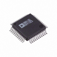
AD8380JSZ Analog Devices Inc, AD8380JSZ Datasheet - Page 9

AD8380JSZ
Manufacturer Part Number
AD8380JSZ
Description
IC DECDRIVER LCD 6CH-OUT 44-MQFP
Manufacturer
Analog Devices Inc
Series
DecDriver™r
Datasheet
1.AD8380JS.pdf
(16 pages)
Specifications of AD8380JSZ
Display Type
LCD
Interface
Parallel
Current - Supply
500µA
Voltage - Supply
9 V ~ 24 V
Operating Temperature
0°C ~ 85°C
Mounting Type
Surface Mount
Package / Case
44-MQFP, 44-PQFP
Lead Free Status / RoHS Status
Lead free / RoHS Compliant
Configuration
-
Digits Or Characters
-
THEORY OF OPERATION
The AD8380 is a system building block designed to directly drive
the columns of poly-silicon LCD panels of the type popular-
ized for use in data projectors. It comprises six channels of
precision 10-bit digital-to-analog converters loaded from a
single, high speed, 10-bit parallel input. Precision current
feedback amplifiers providing well-damped pulse responses
and rapid voltage settling into large capacitive loads buffer the
six outputs. Excellent linearity performance and laser trimming
of scale factors and output offsets at the wafer level ensure low
absolute output errors over all input codes. Tight channel-to-
channel matching in high channel count systems is guaranteed
by reliance on an externally-applied voltage reference.
Transfer Function
The transfer function of the AD8380 is made up of two regions
of operation, in which the video output voltages are either above
or below an output reference voltage externally applied at the
VMID input.
STSQ/CS
VREFLO
DB [0:9]
VREFHI
A[0:2]
STBY
CLK
XFR
BYP
E/O
R/L
(VMID + VFS)
(VMID – VFS)
10
3
VMID
SELECTOR
CONTROL
CHANNEL
SCALING
BIAS
AD8380
0
10
10
10
10
10
10
2-STAGE
2-STAGE
2-STAGE
2-STAGE
2-STAGE
2-STAGE
LATCH
LATCH
LATCH
LATCH
LATCH
LATCH
INV
VOUTN
VOUTP
INPUT CODE
10
10
10
10
10
10
DAC
DAC
DAC
DAC
DAC
DAC
INV = H
INV = L
VMID
1023
VID0
VID1
VID2
VID3
VID4
VID5
The region over which the output voltage varies with input code
is defined by the status of the INV input. When INV is low, the
video output voltages rise from (VMID – VFS), (where VFS =
the full-scale output voltage), to VMID as the input code increases
from 0 to 1023. When INV is high, the output voltages drop
from (VMID + VFS) to VMID with increasing code (see
Figure 4).
For each value of input code there are then two possible values
for the output voltage, depending on the status of INV. When
INV is low the output is defined as VOUTP(N) where N refers
to the input code, and the P refers to the positive slope of the
voltage variation with code. When INV is high, the output is
defined as VOUTN(N).
To best correlate transfer function errors to image artifacts, the
overall accuracy of the AD8380 is defined by comparing the output
voltages, VOUTP(N) and VOUTN(N), to each other and to
their ideal values. Two parameters are defined, one dependent
on the difference between the signal amplitudes at a particular
code, and one dependent on their average value. These are VDE
and VCME. Their defining expressions are:
VDE = [VOUTN(N) – VOUTP(N)]/2 – [(1 – N/1023) × VFS]
where
N = input code, and VFS = 2 × (VREFHI – VREFLO)
VCME = [[VOUTN(N) +VOUTP(N)]/2 – VMID] × (1/2)
where
VMID = midpoint reference voltage for the video outputs.
Setting the Full-Scale Output
The full-scale output voltage (VFS), which defines the maxi-
mum output voltage excursion for a full code input transition, is
defined as twice the voltage difference between the VREFHI and
VREFLO inputs.
Operating Modes, Control Logic and DAC Latches
Control logic included on the AD8380 chip facilitates channel
loading in ascending or descending order (for image mirroring),
data loading on rising or falling clock edges (for even/odd word
loading), and addressing and loading individual channels (for
system testing or debugging). The on-chip logic makes it easy to
build systems requiring more than six drive channels per color.
DAC latches are of a two-stage master-slave design that guaran-
tees all channel outputs are updated simultaneously.
AD8380


