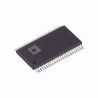
AD8511ARU-REEL Analog Devices Inc, AD8511ARU-REEL Datasheet

IC MUX LCD DVR 11CH 3.3V 48TSSOP

AD8511ARU-REEL

Manufacturer Part Number
AD8511ARU-REEL
Description
IC MUX LCD DVR 11CH 3.3V 48TSSOP
Manufacturer
Analog Devices Inc
Datasheet

Specifications of AD8511ARU-REEL

Rohs Status
RoHS non-compliant
Display Type
LCD
Configuration
64 grey scale
Current - Supply
10mA
Voltage - Supply
3.3 V ~ 6.5 V
Operating Temperature
-40°C ~ 85°C
Mounting Type
Surface Mount
Package / Case
48-TSSOP
Interface
-
Digits Or Characters
-

Available stocks

Company
Part Number
Manufacturer
Quantity
Price
Part Number:
AD8511ARU-REEL
Manufacturer:
SHINILAN
Quantity:
1 828
FEATURES
Single-supply operation: 3.3 V to 6.5 V
High output current: 300 mA
Low supply current: 6 mA
Stable with 1000 pF loads
Pin compatible with LMC6009
Pin compatible with CL-FP6131
48-lead, Pb-free TSSOP/LFCSP packages
APPLICATION
LCD line inversion gamma references
GENERAL DESCRIPTION
The AD8509 and AD8511 are 9-channel and 11-channel LCD
reference buffers, respectively, designed to drive 64 gray scale
column drivers. Each buffer has an A/B input to select between
two voltages for LCD displays. These buffers drive the resistor
ladders of LCD column drivers for gamma correction. The LCD
drivers have higher slew rates and higher output drive currents
than similar competitive parts. This increases the stability of
the reference ladder, resulting in better gray scale and visual
performance.
The AD8509 and AD8511 are specified over the −40°C to +85°C
temperature range. They are available in 48-lead, Pb-free TSSOP
packages in tape and reel. Additionally, the ADD8511 is available
in a 48-lead, Pb-free LFCSP package.
Rev. C
Information furnished by Analog Devices is believed to be accurate and reliable. However, no
responsibility is assumed by Analog Devices for its use, nor for any infringements of patents or other
rights of third parties that may result from its use. Specifications subject to change without notice. No
license is granted by implication or otherwise under any patent or patent rights of Analog Devices.
Trademarks and registered trademarks are the property of their respective owners.
FUNCTIONAL BLOCK DIAGRAM
INA11
INB11
INA1
INB1
INA2
INB2
A/B
Figure 1.
VO1
VO2
VO11
9- and 11-Channel, Muxed Input
One Technology Way, P.O. Box 9106, Norwood, MA 02062-9106, U.S.A.
Tel: 781.329.4700
Fax: 781.461.3113
INA1
INB1
INA2
INB2
INA3
INB3
INA4
INB4
INA5
INB5
INA6
INB6
INA7
INB7
INA8
INB8
INA9
INB9
NC
NC
NC
NC
NC
NC
NC = NO CONNECT
10
11
12
13
14
15
16
17
18
19
20
21
22
23
24
1
2
3
4
5
6
7
8
9
NC = NO CONNECT
Figure 2. AD8509 and AD8511 48-Lead TSSOP (RV Suffix)
(Not to Scale)
INA3
INB3
INA4
INB4
INA5
INB5
INA6
INB6
INA7
INB7
INA8
INB8
AD8509
TOP VIEW
10
12
11
LCD Reference Buffers
1
2
3
4
5
6
7
8
9
PIN CONFIGURATIONS
Figure 3. AD8511 48-Lead LFCSP
48
47
46
45
44
43
42
41
40
39
38
37
36
35
34
33
32
31
30
29
28
27
26
25
PIN 1
INDICATOR
©2006 Analog Devices, Inc. All rights reserved.
NC
NC
NC
NC
V
GND
VO1
VO2
VO3
VO4
V
GND
VO5
VO6
VO7
VO8
VO9
GND
V
A/B
NC
NC
NC
NC
CC
CC
CC
(Not to Scale)
AD8509/AD8511
AD8511
TOP VIEW
INA10
INB10
INA11
INB11
INA1
INB1
INA2
INB2
INA3
INB3
INA4
INB4
INA5
INB5
INA6
INB6
INA7
INB7
INA8
INB8
INA9
INB9
NC
NC
10
11
12
13
14
15
16
17
18
19
20
21
22
23
24
1
2
3
4
5
6
7
8
9
NC = NO CONNECT
(Not to Scale)
AD8511
TOP VIEW
www.analog.com
36
35
34
33
32
31
30
29
28
27
26
25
VO2
VO3
VO4
VO5
V
GND
VO6
VO7
VO8
VO9
VO10
GND
48
47
46
45
44
43
42
41
40
39
38
37
36
35
34
33
32
31
30
29
28
27
26
25
CC
NC
VO1
NC
NC
V
GND
VO2
VO3
VO4
VO5
V
GND
VO6
VO7
VO8
VO9
VO10
GND
V
A/B
NC
NC
VO11
NC
CC
CC
CC

Related parts for AD8511ARU-REEL

AD8511ARU-REEL Summary of contents

Page 1

FEATURES Single-supply operation: 3 6.5 V High output current: 300 mA Low supply current Stable with 1000 pF loads Pin compatible with LMC6009 Pin compatible with CL-FP6131 48-lead, Pb-free TSSOP/LFCSP packages APPLICATION LCD line inversion gamma ...

Page 2

AD8509/AD8511 TABLE OF CONTENTS Features .............................................................................................. 1 Application ........................................................................................ 1 General Description ......................................................................... 1 Functional Block Diagram .............................................................. 1 Pin Configurations ........................................................................... 1 Revision History ............................................................................... 2 Specifications..................................................................................... 3 Electrical Characteristics............................................................. 3 REVISION HISTOR Y 2/06—Rev. C Added LFCSP Package.......................................................Universal ...

Page 3

SPECIFICATIONS ELECTRICAL CHARACTERISTICS 25°C, unless otherwise noted Table 1. Parameter INPUT CHARACTERISTICS Offset Voltage Input Bias Current Voltage Gain OUTPUT CHARACTERISTICS Output Voltage High Output Voltage Low Output Short-Circuit Current POWER SUPPLY ...

Page 4

AD8509/AD8511 ABSOLUTE MAXIMUM RATINGS Table 2. Parameter Rating Supply Voltage 7 V Input Voltage GND to V Storage Temperature Range TSSOP (RV-48) −65°C to +150°C Operating Temperature Range −40°C to +85°C Junction Temperature Range TSSOP (RV-48) Package −65°C to +150°C ...

Page 5

PIN CONFIGURATIONS AND FUNCTION DESCRIPTIONS INA1 4 45 INB1 5 44 INA2 6 43 INB2 7 42 INA3 8 41 AD8509 INB3 9 40 TOP VIEW INA4 (Not to Scale) 10 ...

Page 6

AD8509/AD8511 TYPICAL PERFORMANCE CHARACTERISTICS –35 – TEMPERATURE (°C) Figure 7. Supply Current vs. Temperature AD8509 ...

Page 7

25° LOAD 15pF L 620mV Figure 11. Large Signal Transient Response—Falling 25° 250Ω 15pF L ...

Page 8

AD8509/AD8511 APPLICATIONS The AD8509 and AD8511 are CMOS buffers with A/B inputs that are used to select between two different reference voltages set external resistor ladder. Input bias currents are orders of magnitude less than competitive parts. ...

Page 9

... SEATING PLANE ORDERING GUIDE 1 Model Temperature Range AD8509ARU-REEL −40°C to +85°C 2 AD8509ARUZ-REEL −40°C to +85°C AD8511ARU-REEL −40°C to +85°C 2 AD8511ARUZ-REEL −40°C to +85°C 2 AD8511ACPZ-REEL −40°C to +85°C 1 All models only available in 2,500-piece reels Pb-free part. ...

Page 10

AD8509/AD8511 NOTES Rev Page ...

Page 11

NOTES Rev Page AD8509/AD8511 ...

Page 12

AD8509/AD8511 NOTES ©2006 Analog Devices, Inc. All rights reserved. Trademarks and registered trademarks are the property of their respective owners. C03237-0-2/06(C) Rev Page ...

Related keywords