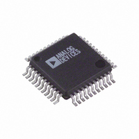
AD8380JS Analog Devices Inc, AD8380JS Datasheet - Page 10

AD8380JS
Manufacturer Part Number
AD8380JS
Description
IC LCD DRIVER 6CH 44-MQFP
Manufacturer
Analog Devices Inc
Series
DecDriver™r
Datasheet
1.AD8380JS.pdf
(16 pages)
Specifications of AD8380JS
Rohs Status
RoHS non-compliant
Display Type
LCD
Interface
Parallel
Current - Supply
500µA
Voltage - Supply
9 V ~ 24 V
Operating Temperature
0°C ~ 85°C
Mounting Type
Surface Mount
Package / Case
44-MQFP, 44-PQFP
Configuration
-
Digits Or Characters
-
Available stocks
Company
Part Number
Manufacturer
Quantity
Price
Company:
Part Number:
AD8380JS
Manufacturer:
HRS
Quantity:
1 600
AD8380
SVGA System Operation
An SVGA system is characterized by the requirement of six
channels of panel drive for each displayed color. Such a system
would use a single AD8380 per color.
With E/O and all address bits A[0:2] set high, channel loading
commences on the first rising edge of CLK following a valid
assertion of the Start Sequence (STSQ) input. The second stage
latches, and therefore the video outputs, are updated on the
first falling edge of the clock following a valid Transfer (XFR)
signal. (See Figure 5 for signal timing details.)
Channel Number
E/O = HIGH
R/L = LOW
Load Sequence Switching (Right/Left Control)
To facilitate image mirroring, the order in which channels are
loaded can be easily switched. When the voltage on the right/left
control input (R/L) is low, the internal sequencer will load data
starting with Channel 0 and counting up to Channel 5. When
this voltage is high, channel loading will be in reverse order, from
Channel 5 down to Channel 0.
XGA System Operation
In an XGA system, twelve column drivers (two AD8380s) are
required for each color (refer to Figure 6). An “even/odd”
system, in which one AD8380 drives even numbered columns
and another drives odd numbered columns, can be easily imple-
mented as detailed in Figures 7 and 8. A clock at one-half the
pixel rate is applied to the CLK input. Even bytes are loaded on
the rising edge of the clock, while odd bytes are loaded on the
falling edge. Identifying whether a chip is to load on rising or falling
edges is done by setting the proper level on the E/O input.
Table I. Sequenced SVGA Data Byte to Channel Assignment
STSQ/CS
DB[0:9]
CLK
XFR
t
3
5
VID0
VID1
VID2
VID3
VID4
VID5
t
4
2.0V
t
7
0
0.8V
t
t
Data Byte Number
0
1
2
3
4
5
1
5
5
t
2
t
6
0
2.0V
t
0.8V
7
O
Channel Number
E/O = HIGH
E/O = LOW
STSQ
STSQ
DB[0:9]
(EVEN
(EVEN
CONTROLLER
CHIP)
CHIP)
CHIP)
CHIP)
(ODD
(ODD
CLK
CLK
XFR
/
/
Table II. Sequenced Even/Odd XGA Data Byte to
Channel Assignment
CLKIN
DB[0:9]
CS
CS
VIDEO
PROCESSOR
PANEL
A0:A2 = HIGH
IMAGE
10
0
DCLK/2
t
STSQ_A
STSQ_B
3
E/O_A
E/O_B
10
VID0
VID1
VID2
VID3
VID4
VID5
VID0
VID1
VID2
VID3
VID4
VID5
1 COLOR OF ‘EVEN/ODD’ XGA
XFR
INV
R/L
t
4
t
3
11
t
4
R/L = LOW
0
2
4
6
8
10
1
3
5
7
9
11
0
Data Byte Number
STSQ/CS
XFR
E/O
R/L
INV
STSQ/CS
XFR
E/O
R/L
INV
9
CLK
CLK
O
t
DEVICE “A”
DEVICE “B”
5
AD8380
AD8380
t
1
10
t
DB[0:9]
DB[0:9]
2
t
6
R/L = HIGH
10
8
6
4
2
0
11
9
7
5
3
1
L
VIDEO
VIDEO
t
A[0:2]
A[0:2]
1
OUT
OUT
11
t
2
DVCC
DVCC
6
6
3
3


