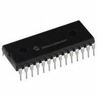
TC835CPI Microchip Technology, TC835CPI Datasheet - Page 12

TC835CPI
Manufacturer Part Number
TC835CPI
Description
IC ADC 4 1/2DGT BCD 28-DIP
Manufacturer
Microchip Technology
Datasheet
1.TC835CKW.pdf
(26 pages)
Specifications of TC835CPI
Display Type
LED
Configuration
7 Segment
Interface
BCD
Digits Or Characters
A/D 4.5 Digits
Current - Supply
1mA
Voltage - Supply
4 V ~ 6 V
Operating Temperature
0°C ~ 70°C
Mounting Type
Through Hole
Package / Case
28-DIP (0.600", 15.24mm)
Lead Free Status / RoHS Status
Lead free / RoHS Compliant
Available stocks
Company
Part Number
Manufacturer
Quantity
Price
Company:
Part Number:
TC835CPI
Manufacturer:
ST
Quantity:
6 217
TC835
6.0
6.1
The integrating resistor is determined by the full-scale
input voltage and the output current of the buffer used
to charge the integrator capacitor. Both the buffer
amplifier and the integrator have a class A output
stage, with 100 µA of quiescent current. A 20 µA drive
current gives negligible linearity errors. Values of 5 µA
to 40 µA give good results. The exact value of an
integrating resistor for a 20 µA current is easily
calculated.
EQUATION 6-1:
6.1.1
The product of integrating resistor and capacitor should
be selected to give the maximum voltage swing that
ensures the tolerance buildup will not saturate the
integrator swing (approximately 0.3V from either
supply). For ±5V supplies and ANALOG COMMON tied
to supply ground, a ±3.5V to ±4V full-scale integrator
swing is adequate. A 0.10 µF to 0.47 µF is
recommended. In general, the value of C
by:
EQUATION 6-2:
A very important characteristic of the integrating
capacitor is that it has low dielectric absorption to
prevent rollover or ratiometric errors. A good test for
dielectric absorption would be to use the capacitor with
the input tied to the reference. This ratiometric
condition should read half scale 0.9999, with any
deviation probably due to dielectric absorption.
Polypropylene capacitors give undetectable errors at
reasonable cost. Polystyrene and polycarbonate
capacitors may also be used in less critical
applications.
DS21478C-page 12
C
INT
TYPICAL APPLICATIONS
Component Value Selection
INTEGRATING CAPACITOR
=
=
R
INT
Integrator output voltage swing
Integrator output voltage swing
(10,000) (clock period) (20
[10,000 x clock period] x I
=
Full scale voltage
20µA
INT
μ
INT
A)
is given
6.1.2
The size of the auto zero capacitor has some influence
on the noise of the system. A large capacitor reduces
the noise. The reference capacitor should be large
enough such that stray capacitance to ground from its
nodes is negligible.
The dielectric absorption of the reference capacitor and
auto zero capacitor are only important at power-on or
when the circuit is recovering from an overload.
Smaller or cheaper capacitors can be used if accurate
readings are not required for the first few seconds of
recovery.
6.1.3
T
output is V
The stability of the reference voltage is a major factor in
the overall absolute accuracy of the converter. For this
reason, it is recommended that a high-quality reference
be used where high-accuracy absolute measurements
are being made.
6.2
6.2.1
A signal integration period at a multiple of the 60Hz line
frequency will maximize 60Hz "line noise" rejection. A
200 kHz clock frequency will reject 60Hz and 400Hz
noise. This corresponds to five readings per second
(see
TABLE 6-1:
he analog input required to generate a full scale
Oscillator Frequency
Table 6-1
Conversion Timing
(kHz)
1200
IN
100
120
200
300
400
800
AUTO ZERO AND REFERENCE
CAPACITORS
REFERENCE VOLTAGE
LINE FREQUENCY REJECTION
= 2V
and
REF
CONVERSION RATE VS.
CLOCK FREQUENCY
Table
.
© 2007 Microchip Technology Inc.
6-2).
Conversion Rate
(Conv./Sec.)
2.5
7.5
10
20
30
3
5


