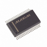
MAX6952EAX+T Maxim Integrated Products, MAX6952EAX+T Datasheet - Page 10

MAX6952EAX+T
Manufacturer Part Number
MAX6952EAX+T
Description
IC DRVR DSPL LED 36-SSOP
Manufacturer
Maxim Integrated Products
Datasheet
1.MAX6952EAX.pdf
(21 pages)
Specifications of MAX6952EAX+T
Display Type
LED
Configuration
5 x 7 (Matrix)
Interface
4-Wire Serial
Digits Or Characters
4 Digits
Current - Supply
12mA
Voltage - Supply
2.7 V ~ 5.5 V
Operating Temperature
-40°C ~ 85°C
Mounting Type
Surface Mount
Package / Case
36-SSOP
Number Of Digits
4
Number Of Segments
140
Low Level Output Current
500 mA
High Level Output Current
50 mA
Operating Supply Voltage
2.7 V to 5.5 V
Maximum Supply Current
16 mA
Maximum Power Dissipation
941.2 mW
Maximum Operating Temperature
+ 85 C
Mounting Style
SMD/SMT
Minimum Operating Temperature
- 40 C
Lead Free Status / RoHS Status
Lead free / RoHS Compliant
4-Wire Interfaced, 2.7V to 5.5V,
4-Digit 5
The S bit in the configuration register selects shutdown
or normal operation (Table 7). The display driver can be
programmed while in shutdown mode, and shutdown
mode is overridden when in display test mode. For nor-
mal operation, the S bit should be set to 1.
The B bit in the configuration register selects the blink
rate. This is the speed that the segments alternate
Table 5. Initial Power-Up Register Status
Table 6. Configuration Register Format
10
Configuration
Register
Intensity10
Intensity32
Scan Limit
Configuration
User-Defined Font
Address Pointer
Display Test
Digit 0 Plane P0
Digit 1 Plane P0
Digit 2 Plane P0
Digit 3 Plane P0
Digit 0 Plane P1
Digit 1 Plane P1
Digit 2 Plane P1
Digit 3 Plane P1
REGISTER
______________________________________________________________________________________
REGISTER
Blink Rate Selection (B Data Bit D2) Format
Shutdown Mode (S Data Bit D0) Format
D7
P
D6
X
✕
7 Matrix LED Display Driver
POWER-UP CONDITION
Address 0x80; pointing to
the first user-defined font
D5
Display 4 digits: 0 1 2 3
R
REGISTER DATA
blink speed is slow,
Shutdown enabled,
Normal operation
Blank digit (0x20)
Blank digit (0x20)
Blank digit (0x20)
Blank digit (0x20)
Blank digit (0x20)
Blank digit (0x20)
Blank digit (0x20)
Blank digit (0x20)
blink disabled
1/16 (min on)
1/16 (min on)
D4
T
location
D3
E
D2
B
D1
X
CODE (HEX)
ADDRESS
D0
S
0x01
0x02
0x03
0x04
0x05
0x07
0x20
0x21
0x22
0x23
0x40
0x41
0x42
0x43
between plane P0 and plane P1 refresh data. The blink
rate is determined by the frequency of the multiplex clock
OSC, in addition to the setting of the B bit (Table 8).
The E bit globally enables or disables the blink feature
of the device (Table 9). When blink is globally enabled,
then the digit data in both planes P0 and P1 are used
to control the display (Table 10).
Table 7. Shutdown Control (S Data Bit D0)
Format
Shutdown
Mode
Normal
Operation
MODE
D7
0
0
X
0
1
X
0
0
0
0
0
0
0
0
D6
0
0
X
X
0
X
0
0
0
0
0
0
0
0
D7
P
P
D5
X
X
0
0
0
0
1
1
1
1
1
1
1
1
D6
X
X
REGISTER DATA
D4
0
0
X
0
0
X
0
0
0
0
0
0
0
0
D5
Global Blink Enable/Disable
R
R
REGISTER DATA
D4
(E Data Bit D3) Format
D3
T
T
0
0
X
0
0
X
0
0
0
0
0
0
0
0
D3
E
E
D2
X
X
0
0
0
0
0
0
0
0
0
0
0
0
D2
B
B
D1
0
0
X
X
0
X
0
0
0
0
0
0
0
0
D1
X
X
D0
D0
0
0
1
0
0
0
0
0
0
0
0
0
0
0
0
1


