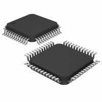
MAX1368ECM+ Maxim Integrated Products, MAX1368ECM+ Datasheet - Page 25

MAX1368ECM+
Manufacturer Part Number
MAX1368ECM+
Description
IC PANEL METER 3.5 DIG 48LQFP
Manufacturer
Maxim Integrated Products
Datasheet
1.MAX1368ECM.pdf
(36 pages)
Specifications of MAX1368ECM+
Display Type
LED
Configuration
7 Segment
Interface
Serial
Digits Or Characters
A/D 3.5 Digits
Voltage - Supply
2.7 V ~ 5.25 V
Operating Temperature
-40°C ~ 85°C
Mounting Type
Surface Mount
Package / Case
48-LQFP
Lead Free Status / RoHS Status
Lead free / RoHS Compliant
Current - Supply
-
Default values:
The overrange register is a 16-bit read/write register (D15
is the MSB). When the conversion result exceeds the
value in the overrange register, the OVER bit in the status
register latches to 1. The LED shows a 1 followed by four
OFFSET_CAL1: (Default = 0.) Automatic offset-calibra-
tion enable bit. When set to 1, the MAX1366/
MAX1368 disable automatic offset calibration. When
this bit is set to zero, automatic offset calibration is
enabled.
SEG_SEL: (Default = 0.) SEG_SEL segment selection
bit. When set to 1, the LED segment drivers use the
LED segment registers to display individual segments
that can form letters or numbers or other information on
the display. The LED data register is not displayed.
Send the data first to the LED segment-display regis-
ters and then set this bit high.
CLR: (Default = 0.) Clear all registers bit. When set to
1, all registers reset to their power-on reset states after
CS makes a low-to-high transition.
RANGE: (Default = 0.) Input range select bit. When set
to zero, the input voltage range is ±2V. When set to 1,
the input voltage range is ±200mV.
PEAK: (Default = 0.) Peak bit. When set to 1 (and the
HOLD bit is set to zero), the LED shows the result
stored in the peak register (see Table 6).
HOLD: (Default = 0.) Hold bit. When set to 1, the LED
register does not update from the ADC conversion
results and holds the last result on the LED. The
MAX1366/MAX1368 continue to perform conversions
during HOLD (Table 1).
PD_ANA: (Default = 0.) Power-down analog select bit.
When set to 1, the analog circuits (analog modulator
and ADC input buffers) go into the power-down mode.
When set to zero, the device is in full power-up mode.
Overrange Register (Read/Write)
MSB
D15
Microcontroller-Interface, 4.5-/3.5-Digit Panel
D14
D13
______________________________________________________________________________________
7CF0h (for 3.5-digit, +1999)
4E1Fh (for 4.5-digit, +19,999)
D12
D11
D10
D9
Meters with 4–20mA Output
D8
PD_DIG: (Default = 0.) Power-down digital select bit.
When set to 1, the digital circuits (digital filter and LED
drivers) go into power-down mode. This also resets the
values of the internal SRAM in the digital filter to zeros.
When set to zero, the device returns to full power-up
mode. When powering down PD_DIG, power down the
LED segment drivers by clearing the ENABLE bit to zero.
DPSET[2:1]: (Default = 00.) Decimal-point selection
bits (Table 2 and 3).
DPON: (Default = 0.) Decimal-point enable bit (Tables
2 and 3).
INTREF: (Default = 0.) Reference select bit. For internal
reference operation, set INTREF to 1. For external refer-
ence operation, set INTREF to zero.
EXTCLK: (Default = 0.) External clock select bit. The
EXTCLK bit controls selection of the internal clock or an
external clock source. A 1 in this location selects the
signal at the CLK input as the clock source. A zero in
this location selects and powers up the internal clock
oscillator.
SPI/ADC: (Default = 0.) Display select bit. The SPI/ADC
bit controls selection of the data fed into LED data reg-
ister. A 1 in this location selects SPI/QSPI/MICROWIRE
data (user writes this data to the LED data register). A
zero in this location selects the ADC result register
data, unless hold or peak functions are active (Table 1).
Note: When changing any one of the following control
bits: OFFSET_CAL1, RANGE, PD_ANA, PD_DIG,
INTREF, and EXTCLK, wait 800ms before reading the
ADC results.
dashes for the MAX1366 or a 1 followed by three dash-
es for the MAX1368 (Table 4).
The data is represented in two’s-complement format.
D7
D6
D5
D4
D3
D2
D1
LSB
D0
25


