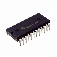
TC14433EPG Microchip Technology, TC14433EPG Datasheet - Page 5

TC14433EPG
Manufacturer Part Number
TC14433EPG
Description
IC ADC 3 1/2 DIGIT 24DIP
Manufacturer
Microchip Technology
Specifications of TC14433EPG
Display Type
LED
Configuration
7 Segment
Interface
BCD
Digits Or Characters
A/D 3.5 Digits
Current - Supply
1.8mA
Voltage - Supply
4.5 V ~ 8 V
Operating Temperature
-40°C ~ 85°C
Mounting Type
Through Hole
Package / Case
24-DIP (0.600", 15.24mm)
Resolution (bits)
3.5bit
Sampling Rate
25SPS
Input Channel Type
Single Ended
Data Interface
BCD
Supply Current
800µA
Digital Ic Case Style
DIP
No. Of Pins
24
Lead Free Status / RoHS Status
Lead free / RoHS Compliant
Available stocks
Company
Part Number
Manufacturer
Quantity
Price
Company:
Part Number:
TC14433EPG
Manufacturer:
MICROCHIP
Quantity:
1 800
Part Number:
TC14433EPG
Manufacturer:
TOSHIBA/东芝
Quantity:
20 000
2.0
The descriptions of the pins are listed in Table 2.0.
©
TABLE 2-1:
(24-Pin CERDIP)
2002 Microchip Technology Inc.
(24-Pin SOIC)
(24-Pin PDIP)
Pin No.
10
11
12
13
14
15
16
17
18
19
20
1
2
3
4
5
6
7
8
9
PIN DESCRIPTIONS
PIN FUNCTION TABLE
(28-Pin PLCC)
Pin No.
10
12
13
14
16
17
18
19
20
21
23
24
11
2
3
4
5
6
7
9
Symbol
R
CLK
CLK
V
EOC
CO
CO
DS
DS
DS
DS
V
V
V
OR
DU
V
Q
R
1
C
REF
AG
EE
SS
/C
X
1
1
0
1
2
4
3
2
1
1
0
1
This is the analog ground. It has a high input impedance. The pin determines the
reference level for the unknown input voltage (V
Reference voltage - Full scale output is equal to the voltage applied to V
Therefore, full scale voltage of 1.999V requires 2V reference and 199.9mV full scale
requires a 200mV reference. V
to V
The unknown input voltage (V
(V
This pin is for external components used for the integration function in the dual
slope conversion. Typical values are 0.1µF (mylar) capacitor for C
R
R
conversion time.
These pins are used for connecting the offset correction capacitor.
The recommended value is 0.1µF.
These pins are used for connecting the offset correction capacitor.
The recommended value is 0.1µF.
Display update input pin. When DU is connected to the EOC output, every
conversion is displayed. New data will be strobed into the output latches during the
conversion cycle if a positive edge is received on DU, prior to the ramp down cycle.
When this pin is driven from an external source, the voltage should be referenced
to V
Clock input pins. The TC14433 has its own oscillator system clock. Connecting a
single resistor between CLK
A crystal or OC circuit may be inserted in lieu of a resistor for improved CLK
clock input, can be driven from an external clock source, which need only have
standard CMOS output drive. This pin is referenced to V
A 300kΩ resistor yields a clock frequency of about 66kHz. See Section 5.0 Typical
Characteristics. (Also see Figure 4-3 for alternate circuits.)
Negative power current. Connection pin for the most negative supply. Please note
the current for the output drive circuit is returned through V
current is 0.8mA.
Negative power supply for output circuitry. This pin sets the low voltage level for the
output pins (BCD, Digit Selects, EOC, OR). When connected to analog ground, the
output voltage is from analog ground to V
is from V
V
End of conversion output generates a pulse at the end of each conversion cycle.
This generated pulse width is equal to one half the period of the system clock.
Overrange pin. Normally this pin is set high. When V
Digit select pin. The digit select output goes high when the respective digit is
selected. The MSD (1/2 digit turns on immediately after an EOC pulse).
The remaining digits turn on in sequence from MSD to LSD.
To ensure that the BCD data has settled, an inter digit blanking time of two clock
periods is included.
Clock frequency divided by 80 equals multiplex rate. For example, a system clock of
60kHz gives a multiplex rate of 0.8kHz.
See Figure 4-4 for digit select timing diagram.
DD
1
1
REF
= 470kΩ (resistor) for 2V full scale.
= 27kΩ (resistor) for 200mV full scale. Clock frequency of 66kHz gives 250msec
EE
SS
-3 volts and V
) in a rationetric A/D conversion.
, the system is reset to the beginning of the conversion cycle.
.
EE
to V
DD
EE
. The recommended operating range for V
.
1
X
and CLK
REF
) is measured as a ratio of the reference voltage
functions as system reset also. When switched
Description
0
sets the clock frequency.
DD
. If connected to V
X
) and the reference voltage (V
TC14433/A
X
exceeds V
EE
for external clock inputs.
SS
SS
. Typical supply
EE
is between the
, the output swing
REF
DS21394B-page 5
1
.
the OR is low.
REF
.
1
, the
REF
).


