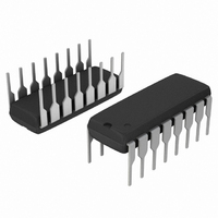
MC14511BCPG ON Semiconductor, MC14511BCPG Datasheet - Page 2

MC14511BCPG
Manufacturer Part Number
MC14511BCPG
Description
IC LATCH/DECODER/DRIVER 16DIP
Manufacturer
ON Semiconductor
Datasheet
1.MC14511BCPG.pdf
(10 pages)
Specifications of MC14511BCPG
Configuration
7 Segment
Interface
BCD
Current - Supply
10µA
Voltage - Supply
3 V ~ 18 V
Operating Temperature
-55°C ~ 125°C
Mounting Type
Through Hole
Package / Case
16-DIP (0.300", 7.62mm)
Product
Decoder / Demultiplexer
Logic Family
MC14
Supply Voltage (max)
18 V
Supply Voltage (min)
3 V
Maximum Operating Temperature
+ 125 C
Minimum Operating Temperature
- 55 C
Mounting Style
Through Hole
Power Dissipation
500 mW
Lead Free Status / RoHS Status
Lead free / RoHS Compliant
Display Type
-
Digits Or Characters
-
Lead Free Status / Rohs Status
Lead free / RoHS Compliant
Other names
MC14511BCPGOS
Available stocks
Company
Part Number
Manufacturer
Quantity
Price
Part Number:
MC14511BCPG
Manufacturer:
ON/安森美
Quantity:
20 000
However, it is advised that normal precautions be taken to avoid application of any voltage higher than maximum rated voltages
to this high−impedance circuit. A destructive high current mode may occur if V
V
to V
SS
This device contains protection circuitry to protect the inputs against damage due to high static voltages or electric fields.
Due to the sourcing capability of this circuit, damage can occur to the device if V
Unused inputs must always be tied to an appropriate logic voltage level (e.g., either V
SS
v (V
and are at a logical 1 (See Maximum Ratings).
in
or V
out
) v V
DD
X = Don’t Care
* Depends upon the BCD code previously applied when LE = 0
LE BI LT
.
X
X
0
0
0
0
0
0
0
0
0
0
0
0
0
0
0
0
1
X
0
1
1
1
1
1
1
1
1
1
1
1
1
1
1
1
1
1
0
1
1
1
1
1
1
1
1
1
1
1
1
1
1
1
1
1
1
Inputs
D
X
X
X
0
0
0
0
0
0
0
0
1
1
1
1
1
1
1
1
0
C
X
X
X
0
0
0
0
1
1
1
1
0
0
0
0
1
1
1
1
1
B
X
X
0
0
1
1
0
0
1
1
0
0
1
1
0
0
1
1
X
V
LE
2
LT
SS
BI
PIN ASSIGNMENT
B
C
D
A
http://onsemi.com
A
X
X
X
0
1
0
1
0
1
0
1
0
1
0
1
0
1
0
1
TRUTH TABLE
3
1
2
3
4
5
6
7
8
DISPLAY
a
1
0
1
0
1
1
0
1
0
1
1
1
0
0
0
0
0
0
4
2
5
b
1
0
1
1
1
1
1
0
0
1
1
1
0
0
0
0
0
0
16
15
14
13
12
10
11
9
6
c
1
0
1
1
0
1
1
1
1
1
1
1
0
0
0
0
0
0
V
f
g
a
b
c
d
e
DD
7
d
1
0
1
0
1
1
0
1
1
0
1
0
0
0
0
0
0
0
*
e
f
8
Outputs
e
1
0
1
0
1
0
0
0
1
0
1
0
0
0
0
0
0
0
d
g
a
9
in
1
0
1
0
0
0
1
1
1
0
1
1
0
0
0
0
0
0
f
c
and V
DD
b
g
1
0
0
0
1
1
1
1
1
0
1
1
0
0
0
0
0
0
is applied, and the outputs are shorted
SS
out
Display
Blank
Blank
Blank
Blank
Blank
Blank
Blank
or V
are not constrained to the range
8
0
1
2
3
4
5
6
7
8
9
*
DD
).


