ZXCT1032N8TA Diodes Zetex, ZXCT1032N8TA Datasheet
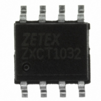
IC CURRENT MONITOR 8SOIC

ZXCT1032N8TA

Manufacturer Part Number
ZXCT1032N8TA
Description
IC CURRENT MONITOR 8SOIC
Manufacturer
Diodes Zetex
Datasheet

Specifications of ZXCT1032N8TA

Function
Current Monitor
Sensing Method
High-Side
Voltage - Input
9.5 ~ 21 V
Operating Temperature
-40°C ~ 85°C
Mounting Type
Surface Mount
Package / Case
8-SOIC (3.9mm Width)
Lead Free Status / RoHS Status
Lead free / RoHS Compliant
Current - Output
-
Accuracy
-
Other names
ZXCT1032N8TR
ZXCT1032
High-side inrush controller and electronic fuse
Description
The ZXCT1032 is a high-side current monitor
that drives a PMOS or PNP transistor to
provide in-rush current limit and over-current
protection. The ZXCT1032 includes a high
accuracy high-side current monitor, a start-up
timer and a re-try inhibit timer.
The ZXCT1032 takes the voltage developed
across a current shunt resistor and compares
this with an externally set trip point. It works
in three modes:
Linear soft-start
Upon power up the ZXCT1032 enters a linear
soft-start mode. During which the output
current ramps up from zero to a maximum
user defined trip point. The trip point is set by
the voltage on I
The ramp rate is determined by capacitor C
The soft start ensures that capacitive loads are
smoothly charged without causing excessive
power supply startup transients.
Over-current detectior
When external capacitor CT has charged up
above the V
soft-start mode to its over-current detection
mode. During this mode the external MOSFET
will be fully enhanced reducing the its voltage
drop and power dissipation.
Features
Ordering information
Issue 4 - June 2007
© Zetex Semiconductors plc 2007
Order code
ZXCT1032N8TA
Linear soft-start
Over-current detector
Over-current disconnect/fuse
Accurate high-side current sensing
User defined and dynamically adjustable
trip current
Load switch control
Fault flag logic output
User defined ramp and inhibit timers
SO8 package
Temperature range -40 to 85°C
ISET
the ZXCT1032 switches from its
SET
pin and R
Pack
SO8
SENSE
Part mark
1032
.
T
.
Reel size
1
While in this mode the internal current monitor
continually checks the output current and
compares it to the trip-current level determined
by V
Over-current disconnect/fuse
If the trip current limit is exceeded at any time the
ZXCT1032 enters its Over-current disconnect
mode. The drive pin is driven high, turning the
pass MOSFET off; the flag output goes low
indicating a fault.
The drive and flag outputs are latched in these
states for a period determined by C
internally set discharge current (3µA typical). After
C
restart into its linear soft-start mode.
The C
ratioed to so that the power dissipation in the
pass MOSFET should allow indefinite operation
in the event of a continuous load failure.
Pin 3 description:
Determines the load current trip level or
constant current level. ISET can be left open
circuit (internal 2.1V reference) or driven via a
DC voltage or µC PWM output. Its source
impedance is 50k .
Applications
7”
T
Electronic fuse
Short circuit protected supply feed
Hot swap
Power over twisted pair
has discharged to 80mV the ZXCT1032 will
ISET
T
charge and discharge times have been
.
Tape width
12mm
Quantity per reel
www.zetex.com
T
500
, V
ISET
and the

Related parts for ZXCT1032N8TA

ZXCT1032N8TA Summary of contents

Page 1

... SO8 package • Temperature range -40 to 85°C Ordering information Order code Pack ZXCT1032N8TA SO8 Issue 4 - June 2007 © Zetex Semiconductors plc 2007 While in this mode the internal current monitor continually checks the output current and compares it to the trip-current level determined by V ...

Page 2

Typical application circuit SENSE 8 IN+ ZXCT I SET 1032 3 C GND µC GND Pin description Pin Name Description 1 GND Ground reference for I device. No other pin should go ...

Page 3

Absolute maximum ratings (a) V max ...................................................................................................... 28 V IN+ Voltage on any pin relative to GND ............................................................. -0.6V and V Maximum differential voltage between V Junction temperature range ........................................................................ -40 to 150°C Storage temperature range .......................................................................... -55 to 150°C ...

Page 4

Typical characteristics (T = 25°C and V = 20V unless otherwise stated) A IN+ Quiescent current vs temperature 0. 9.5 to 21V IN+ 0.60 0.30 0.00 -40 -15 10 Temperature ( temperature ISET 2.20 2.15 2.10 ...

Page 5

Typical characteristics (T = 25°C and V = 20V unless otherwise stated temperature CT-CHG 0 -25 -50 -75 -100 -125 -150 -175 -200 -225 -250 -40 -15 10 Temperature (° temperature CT-DIS 5.0 4.5 ...

Page 6

Application information ZXCT1032 block diagram and description R SENSE (8) IN+ I CT-CHG 200 A (3) I SET ( DIS - 3 GND (1) Operation of the ZXCT1032 1 After power-up, the ...

Page 7

The output voltage also increases due to the load current powering up the load and charging any capacitance. After the initial soft start (load current stabilizing) the timing capacitor charges and the device enters its normal ...

Page 8

When C has discharged to "zero" (< 80mV) the latch is reset which re-enables the output drive T and allows the device to re-enter soft-start mode the event of an overload or short circuit, stages 3 and ...

Page 9

Package outline - SO8 DIM Inches Min. Max. A 0.053 0.069 A1 0.004 0.010 D 0.189 0.197 H 0.228 0.244 E 0.150 0.157 L 0.016 0.050 Note: Controlling dimensions are in inches. Approximate dimensions are provided in millimeters Issue 4 ...

Page 10

Definitions Product change Zetex Semiconductors reserves the right to alter, without notice, specifications, design, price or conditions of supply of any product or service. Customers are solely responsible for obtaining the latest relevant information before placing orders. Applications disclaimer The ...

Related keywords