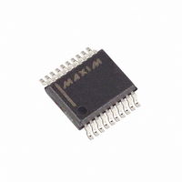
MAX1667EAP+ Maxim Integrated Products, MAX1667EAP+ Datasheet - Page 2

MAX1667EAP+
Manufacturer Part Number
MAX1667EAP+
Description
IC SMART BATT CHGR LEVEL2 20SSOP
Manufacturer
Maxim Integrated Products
Datasheet
1.MAX1667EAPT.pdf
(26 pages)
Specifications of MAX1667EAP+
Function
Charge Management
Battery Type
All Battery Types
Voltage - Supply
7.5 V ~ 28 V
Operating Temperature
-40°C ~ 85°C
Mounting Type
Surface Mount
Package / Case
20-SSOP
Lead Free Status / RoHS Status
Lead free / RoHS Compliant
ABSOLUTE MAXIMUM RATINGS
DCIN to AGND .......................................................-0.3V to +30V
BST to AGND..........................................................-0.3V to +36V
BST, DHI to LX..........................................................-0.3V to +6V
LX, IOUT to AGND..................................................-0.3V to +30V
THM, CCI, CCV, DACV, REF,
VL, SEL, INT, SDA, SCL to AGND ............................-0.3V to +6V
BATT, CS+ to AGND ..............................................-0.3V to +20V
ELECTRICAL CHARACTERISTICS
(V
are at T
Chemistry-Independent,
Level 2 Smart Battery Charger
Stresses beyond those listed under “Absolute Maximum Ratings” may cause permanent damage to the device. These are stress ratings only, and functional
operation of the device at these or any other conditions beyond those indicated in the operational sections of the specifications is not implied. Exposure to
absolute maximum rating conditions for extended periods may affect device reliability.
2
SUPPLY AND REFERENCE
SWITCHING REGULATOR
DCIN Input Voltage Range
DCIN Quiescent Current
VL Output Voltage
VL Load Regulation
VL AC_PRESENT Trip Point
REF Output Voltage
Oscillator Frequency
DHI Maximum Duty Cycle
DHI On-Resistance
DLO On-Resistance
BATT Input Current (Note 1)
CS Input Current (Note 1)
BATT, CS Input Voltage Range
CS to BATT Single-Count
Current-Sense Voltage
CS to BATT Full-Scale
Current-Sense Voltage
Voltage Accuracy
DLO to AGND .............................................-0.3V to (VL + 0.3V)
DCIN
_______________________________________________________________________________________
= 18V, internal reference, 1µF capacitor at REF, 1µF capacitor at VL, T
A
= +25°C, unless otherwise noted.)
PARAMETER
7.5V < V
7.5V < V
I
0 < I
Not in dropout
In dropout
High or low
High or low
VL < 3.2V, V
VL > 5.15V, V
VL < 3.2V, V
VL > 5.15V, V
ChargingCurrent() = 0x0080 (128mA)
SEL = VL (4A),
ChargingCurrent() = 0x0F80 (3968mA)
ChargingVoltage()
= 0x3130 (12,592mV)
and
0x41A0 (16,800mV)
ChargingVoltage()
= 0x1060 (4192mV)
and
0x20D0 (8400mV)
LOAD
SOURCE
= 0 to 10mA
DCIN
DCIN
BATT
CS
< 500µA
BATT
CS
< 28V, logic inputs = VL
< 28V, no load
= 12V
= 12V
= 12V
CONDITIONS
= 12V
T
T
T
T
A
A
A
A
PGND to AGND .....................................................-0.3V to +0.3V
SDA, INT Current ................................................................50mA
VL Current ...........................................................................50mA
Continuous Power Dissipation (T
Operating Temperature Range ...........................-40°C to +85°C
Storage Temperature Range .............................-60°C to +150°C
Lead Temperature (soldering, 10s) .................................+300°C
= T
= T
SSOP (derate 8mW/°C above +70°C) ..........................640mW
= +25°C
= +25°C
MIN
MIN
A
to T
to T
= 0°C to +85°C, unless otherwise noted. Typical values
MAX
MAX
4.055
5.15
3.20
96.5
MIN
-0.8
-1.0
-1.0
-3.0
200
145
7.5
0
A
= +70°C)
4.096
TYP
97.7
250
350
170
160
5.4
4
4
4
5
1
1
5
4.137
MAX
5.65
5.15
100
300
500
400
175
0.8
1.0
1.0
3.0
28
19
6
7
8
5
5
UNITS
kHz
mA
mV
mV
mV
µA
µA
%
%
Ω
Ω
V
V
V
V
V


