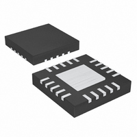
MAX17435ETG+T Maxim Integrated Products, MAX17435ETG+T Datasheet - Page 26

MAX17435ETG+T
Manufacturer Part Number
MAX17435ETG+T
Description
IC SMBUS BATT CHARGER 24TQFN
Manufacturer
Maxim Integrated Products
Datasheet
1.MAX17435ETG.pdf
(28 pages)
Specifications of MAX17435ETG+T
Function
Charge Management
Battery Type
Multi-Chemistry
Voltage - Supply
8 V ~ 26 V
Operating Temperature
-40°C ~ 85°C
Mounting Type
Surface Mount
Package / Case
24-TQFN Exposed Pad
Lead Free Status / RoHS Status
Lead free / RoHS Compliant
High-Frequency,
Low-Cost SMBus Chargers
Inductor L1 must have a saturation current rating of at
least the maximum charge current plus 1/2 the ripple
current (DI
The ripple current is determined by:
where:
or:
The input capacitor must meet the ripple current
requirement (I
Nontantalum
OS-CON) are preferred due to their resilience to power-
up surge currents:
The input capacitors should be sized so that the
temperature rise due to ripple current in continuous
conduction does not exceed approximately 10NC. The
maximum ripple current occurs at 50% duty factor or
V
application of interest does not achieve the maximum
value, size the input capacitors according to the worst-
case conditions.
The output capacitor absorbs the inductor ripple current
and must tolerate the surge current delivered from the
battery when it is initially plugged into the charger.
As such, both capacitance and ESR are important
parameters in specifying the output capacitor as a filter
and to the ensure stability of the DC-DC converter. See the
Compensation section. Beyond the stability requirements,
it is often sufficient to make sure that the output capacitor’s
ESR is much lower than the battery’s ESR. Either tantalum
or ceramic capacitors can be used on the output.
Ceramic devices are preferable because of their good
26
DCIN
_____________________________________________________________________________________
= 2 x V
I
RMS
t
L
OFF
):
V
t
OFF
=
RMS
DCIN
BATT
= 0.3Fs for V
chemistries
I
I
CHG
SAT
DI
= 2.5Fs (V
) imposed by the switching currents.
, which equates to 0.5 x I
L
for V
Output Capacitor Selection
= I
= V
Input Capacitor Selection
CHG
V
BATT
BATT
BATT
BATT
DCIN
+ (1/2) DI
(ceramic,
< 0.88 V
O t
(
V
V
DCIN
DCIN
OFF
> 0.88 V
- V
/L
BATT
- V
DCIN
L
BATT
aluminum,
DCIN
)/
CHG
)
. If the
or
voltage ratings and resilience to surge currents. For most
applications the output capacitance can be as low as
4.7FF. If the output voltage is low and the input voltage is
high, the output capacitance may need to be increased.
Bypass DCIN with a 0.1FF ceramic to ground (Figure 1).
N3 and Q1A protect the MAX17435/MAX17535 when the
DC power source input is reversed. Bypass V
LDO, and V
Good PCB layout is required to achieve specified noise
immunity, efficiency, and stable performance. The
PCB layout artist must be given explicit instructions—
preferably, a sketch showing the placement of the power
switching components and high current routing. Refer
to the PCB layout in the MAX17435 and MAX17535
Evaluation Kits for examples. A ground plane is essential
for optimum performance. In most applications, the circuit
is located on a multilayer board, and full use of the four or
more copper layers is recommended. Use the top layer
for high current connections, the bottom layer for quiet
connections, and the inner layers for an uninterrupted
ground plane.
Use the following step-by-step guide:
1) Place the high-power connections first, with their
grounds adjacent:
U Minimize the current-sense resistor trace lengths,
U Minimize ground trace lengths in the high-current
U Minimize other trace lengths in the high-current
U Use > 5mm wide traces in the high-current paths.
U Connect C1 and C2 to high-side MOSFET (10mm
U Minimize the LX node (MOSFETs, rectifier cathode,
and ensure accurate current sensing with Kelvin
connections.
paths.
paths.
max length).
inductor (15mm max length). Keep LX on one side
of the PCB to reduce EMI radiation.
AA
, as shown in Figure 1.
Applications Information
Layout and Bypassing
CC
, DCIN,


